Brian Klene and Daniel J. Colon III
Light source manufacturers move away from the single gas discharge chamber to a new design that meets the increasing demands of semiconductor processing.
The use of deep-UV
excimer light sources in semiconductor chip manufacturing has grown dramatically
in the last five years. More than half of the lithography exposure systems shipped
since 2000 employ these devices as illumination sources. While their application
to semiconductor processing has enabled the industry to pattern microelectronic
circuits at 0.25 μm and below, a number of developing trends will significantly
affect their use and complexity.
As with all other process equipment used in semiconductor
manufacturing, Moore’s law — which states that the number of transistors
per square inch on integrated circuits doubles every 18 months — is the fundamental
driver for light source technology. The need to shrink the dimensions of wafer patterns
further is limited by the ability to optically resolve two adjacent features.
The imaging performance of a lithography
system is defined by the Rayleigh equation, where resolution = k1 x wavelength/numerical
aperture. The light source affects all three components of the equation. As its
emitted wavelength decreases, so does the attainable critical dimension on the wafer.
Lithographers are interested in using excimer light sources capable of emitting
increasingly shorter wavelengths.
Lens designers seek to use increasingly
higher numerical apertures in their lithography exposure tools to improve resolution,
but high-numerical-aperture lenses need very nearly monochromatic light, which requires
a deep-UV excimer light source to emit an increasingly narrow spectral bandwidth.
The k1 factor is related to the imaging process and resolution-enhancement techniques.
In many cases, deep subwavelength patterning is nearly impossible without enhancement,
and deep-UV excimer lasers can be used to optimize the performance of those techniques.
Several of other trends are affecting
excimer light source development. Shrinking semiconductor design rules and process
windows, coupled with the transition to 300 mm and higher throughput requirements,
have resulted in a demand for excimer light sources that deliver high spectral purity
and power, and dose and wavelength stability. These sources will provide dose uniformity
and focus stability at the wafer plane, as well as adequate throughput.
Manufacturing improvements
The industry’s push to lower costs will
also affect manufacturers. Improvement in spectral bandwidth performance will
allow lithographers to use not only high-numerical-aperture lens designs, but also
fewer elements made of CaF2, which is not readily available. Higher power levels
will enable lithography tools to achieve a very high wafer throughput, even when
using many optically inefficient resolution-enhancement techniques. This is essential
because lithographers want to optimize their investment in deep-UV equipment by
extending production as much as possible before investing in new, shorter-wavelength
technologies.
Up until now, light sources for photolithography
have been using a single gas discharge chamber design, where the single chamber
works with complementary optical components to generate light at tight spectral
bandwidths and high output power. This type of light source can be optimized for
bandwidth or output power, but not both.
To improve capabilities in terms of
both spectral bandwidth and output power, excimer light source manufacturers must
make the transition from the single-chamber design to a new dual-chamber design
called master oscillator power amplifier (see figure). One chamber optimizes bandwidth
performance, and the second optimizes power generation. As a result, light sources
based on this design will not encounter the inherent limitations of using a single
chamber for future needs.
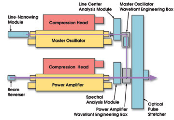
The master oscillator power amplifier architecture consists of two
chambers vertically integrated on an optical table. Each chamber is attached to
a compression head. Optical module subsystems, shown in aqua, provide a variety
of functions, such as line narrowing, metrology, beam propagation and optical pulse
stretching.
These trends also will affect the industry’s
selection of deep-UV excimer light sources. The main DUV sources currently used
in production are those that employ the gas krypton fluoride (KrF), which emits
at 248 nm. KrF light sources are sufficient for enabling lithography tools to image
features ranging down to approximately 0.13 μm. Lithographers, however, will
want to extend these light sources as much as possible through resolution-enhancement
techniques and master oscillator power amplifier technologies. This will result
in KrF remaining the dominant production exposure wavelength for the next three
to four years.
But as the industry follows the International
Technology Roadmap for Semiconductors and begins the transition to nodes with resolution
of 100 nm and lower, KrF will eventually reach its imaging performance limits at
critical layers, and the industry will turn to argon-fluoride (ArF) technology to
meet its production requirements. ArF emits at 193 nm, which will enable lithography
tools to image features at lower-resolution nodes, and the adoption of master oscillator
power amplifier technology will enable excimer light source manufacturers to meet
future requirements.
ArF technology will gradually increase
its share of deep-UV-wavelength production between now and 2006, at which time it
is expected to overtake KrF in volume production. After that, shorter-wavelength
technology, such as F2 (157 nm) and extreme-UV (13.5 nm) will vie for production
dominance. Both of these technologies, however, are still in the development phase.
Meet the authors
Brian Klene is executive vice president of Cymer
Inc.’s emerging technology and applications business unit in San Diego.
Daniel J. Colon III is senior released
products marketing manager at Cymer.