While the US remains a hot spot for development of microtechnology, European firms appear to be building up for a potential market lead.
Nadya Anscombe, Contributing Editor
Nanotechnology may be the latest buzzword, but its predecessor — microtechnology — has yet to reach its full potential. Although much hype is being made of the idea of nanomachines, researchers around the world are still trying to make micromachines a reality. Microelectromechanical systems (MEMS), also called microsystems in Europe and micromachines in Japan, essentially are still emerging technologies.
Photonics-related MEMS technology, for example, is diverse in function and scope, crossing a variety of application areas from telecom to biomedicine. Photonic devices such as optical switches could be stand-alone MEMS devices or components within more-complex ones. Or MEMS could be subsystems of photonic devices, such as the 320 × 240 MEMS-based uncooled IR detector engine recently introduced by Sarnoff Corp. in Princeton, N.J. According to its designers, the device captures images with an array of heat-sensitive microscopic cantilever elements machined into its surface, one for each pixel. As the elements bend in response to heat from the IR radiation, they generate electrical signals to create a thermal image.
Such potential across all categories of MEMS devices is fueling growth of the global market, which was estimated at roughly $3.5 billion for 2002 (the silicon portion of MEMS chips only) by Yole Développement of Lyon, France. The consultancy expects compound annual growth for 2002 through 2005 to average about 25 percent, with segments such as gyros making stronger gains than accelerometers, pressure sensors and ink-jet heads (see bar chart).
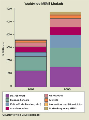
Yole Développement recently analyzed 368 MEMS fabrication facilities worldwide. Its report estimated an average compound annual growth in the market of 25 percent through 2005, with devices such as accelerometers, pressure sensors and ink-jet heads averaging roughly 15 percent growth.
This is fairly healthy growth compared with the depressed semiconductor and photonics markets, though, and is an indication of the huge potential that MEMS still hold.
Based on the findings of its March 2003 “World MEMS Fab” report, Yole claims that there are roughly 368 MEMS fabrication facilities worldwide, most of them with an average of 25 employees. It estimates that there are more than 130 MEMS applications in production today, very few of them involving high-volume products such as ink-jet heads, pressure sensors and acceleration sensors. Potential new applications in the medical, biotechnical and instrumentation fields also could contribute to the predicted growth.
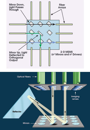
A two-dimensional MEMS cross connect (above) uses a matrix of hinged micromirrors to route light signals from an array of input fibers to an array of output fibers. In three-dimensional devices (below), the micromirrors are under analog control, tilting freely on two planes to route the light in 3-D space. Courtesy of Yole Développement.
North America has the largest number of MEMS companies, but when Yole focused on those worldwide with more than 10 employees, it found that almost 46 percent were European. Even though the North American MEMS industry is more mature, Europe is apparently closing the gap fast, threatening to overtake its cousin across the Atlantic.
Some industry observers believe this is because European governments have made a concerted effort to invest in MEMS development and because of the number of collaborative networks that exist across the region. These include Nexus, a not-for-profit organization that aims to provide MEMS professionals with access to information and networking opportunities, and Europractice, a collection of projects funded by the European Commission to enable the complete supply chain for MEMS.
“Europractice is a very interesting initiative that helps companies to get access to tools that are important for the dissemination of MEMS know-how,” said Jean-Christophe Eloy, Yole’s director.
Cooperation in Europe is important to MEMs companies because many of them still have relatively small production volumes. Another difference, according to Eloy, is that many smaller European firms target niche markets with high added value. “This is because these companies are usually spin-outs from research institutes and were set up to solve a particular problem,” he said.
In Asia, the picture is very different. Japan, for instance, has very few cohesive regional research efforts, and MEMS commercialization is handled mainly by a handful of large electronics companies. There is no start-up culture as in Europe and the US. However, this is not the case in South Korea, where there are several start-ups. In Taiwan, several foundries have made investments in the technology, and China also is investing in MEMS research and commercialization.
In North America, more of the larger semiconductor companies dominate the market, but the European semiconductor manufacturers are starting to make inroads. Infineon Technologies AG in Munich, Germany, recently purchased MEMS manufacturer SensoNor in Horton, Norway, and STMicroelectronics in Geneva set up its own MEMS business unit. Other semiconductor companies investing in the technology include Austria Mikro Systeme International AG of Unterpremstätten, Austria, and Semefab in Glen?rothes, UK.
The open foundry business model is reportedly much more popular in Europe than in North America, where there are more systems manufacturers with internal MEMS production. North American companies tend to process more 8-inch wafers because of higher-volume production demands.
Some believe that the European MEMS industry has the lead in polymer technology, but, in general, the market is quite fragmented, with a few high-volume applications, especially ink-jet heads. However, there is a growing market for microfluidics and other bio-related arrays. “Europe is service-oriented in microfluidics,” Eloy said. “Polymer microreplication is emerging very strongly, and there is a strong presence in DNA microarrays and protein arrays.”
Waiting for recovery
In optics, the situation is a little bleaker. Eloy said that most companies are merely trying to stay alive so that their products will be on the market when the optics and telecom industries recover. “Many companies are investing heavily in R&D for optics components such as micro-optical silicon benches, switches and new, innovative devices,” he said. Several foundries are also investing in new equipment, including Silicon Sensing Systems Ltd. in Plymouth, UK; Memscap in Bernin, France; Tronic’s Microsystems SA in Crolles, France; and Silex Microsystems AB in Järfälla, Sweden.
As with all industries connected with the semiconductor and telecommunications markets, the MEMS industry has had casualties. Many innovative companies on both sides of the Atlantic have disappeared, with North America taking the hardest hit. “In the US, start-up companies tend to grow very quickly, but this also means they tend to fold very quickly,” Eloy said. “Many European firms are managing to survive and are holding out for an upturn in the telecom and semiconductor markets.”
And he believes that further consolidation is inevitable. Besides start-ups going out of business, companies continue to be bought up by others. For example, in 2002, Memscap laid claim to JDS Uniphase’s MEMS business, Cronos, in San Jose, Calif., and in late 2001 it acquired Capto AS in Skopum, Norway, which has since become its Sensor Solutions Business Unit. In October, the company purchased Opsitech in Grenoble, France, which specializes in integrated optics that can be associated with MEMS.
Pure-play MEMS
Memscap is now one of Europe’s largest MEMS companies and the only pure-play MEMS company to be listed on a stock exchange (Euronext). As is true with all companies in this field, it has been through tough times. But, after some severe rationalization and diversification, it reportedly is still going strong. Its third-quarter results for 2003 are encouraging: Revenue was €1.9 million, compared with €1.3 million for the same period in 2002. The company reports that revenues for the first three quarters of 2003 already equal total revenues reported in 2002.
CEO Jean-Michel Karam is confident that Memscap will return to profitability in 2004: “When we started in 1998, we concentrated mainly on optical products. Year 2001 was a fantastic year, with revenue as high as $179 million. But we realized the downturn was coming and decided to diversify into the biomedical and aerospace business by buying Capto in 2001. The next year was disastrous — even the sensor business suffered. We went from being 269 people to 180 today, and we are beginning to see business picking up again, even in the telecom industry. The hardest times are now behind us, and we aim to be profitable again in 2004.”
One product that could help Memscap achieve this target is a closed-loop digital variable optical attenuator that it is developing with recently acquired GalayOr Inc. in Tel Aviv, Israel, a provider of all-silicon optical systems on a chip. The company plans to send samples to no more than 25 companies, with volume production planned for sometime next year.
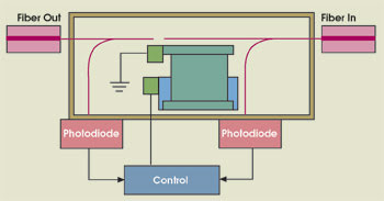
This MEMS-based digital variable optical attenuator, developed by Memscap and two other firms, integrates the functionalities of several optical and electronic components. The structure in the middle represents the one-dimensional MEMS actuator that moves one waveguide, changing the coupling efficiency between the input and the output waveguide.
The device, which was jointly developed with GalayOr and Analog Devices of Norwood, Mass., integrates the functionalities of several optical and electronic discrete components into a single module measuring 42 × 17 × 10 mm. It allows onboard microprocessor control, alarm reporting, onboard input/output optical power monitoring, automatic calibration and optical automatic power control with continuous adjustment to environmental changes and aging.
The core technology of the attenuator consists of moving silicon waveguides. To perform functions such as attenuation, switching, filtering or alignment, MEMS shift these waveguides in and out of the silicon plane. GalayOr claims it has broken the traditional coupling barrier of silicon to fibers, achieving a coupling efficiency better than 90 percent (0.3-dB coupling loss).
The device will be made in Memscap’s new fabrication facility. “We started construction in June 2001, and by June 2002, we were shipping the first fully qualified products,” Karam said.
Large Investment
Also investing heavily in manufacturing capability is Silex. An example of a European company set up by academic researchers, Silex recently invested in a new production facility in Järfälla. This announcement follows the closing of the company’s second round of financing, which attracted €7.7 million from investors.
The company recently signed a lease contract with Zarlink Semiconductor encompassing 450 square meters of cleanroom area and 500 square meters of office space within Zarlink’s Järfälla premises. It is building a full 6-inch-wafer MEMS production line in an existing cleanroom that it expects to be fully operational by year’s end.
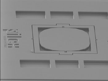
MEMS micromirrors could be the optical switching technology of the future. Courtesy of Silex Microsystems.
Silex specializes in the life sciences and telecommunications markets. Examples of its products include disposable blood pressure sensors, general substrates for optical components and movable mirror arrays for imaging and optical fiber switching. CEO Jan Nerdal agrees with Karam that there is light at the end of the tunnel. “Our telecom and optical customers are preparing themselves for an upturn in the market,” he said. “They are investing.”
So with a predicted average annual growth rate of 25 percent in the near term, consolidation still in process and serious investment going on, the European MEMS industry appears to be gaining strength. It seems that demand for microtechnology can only continue to grow as end users explore its potential.
Useful Web Sites on the European MEMS Industry
Nexus
www.nexus-mems.com
A not-for-profit organization that provides access to information and to networking opportunities for MEMS professionals.
Europractice
www.europractice.com and www.microsystems-suppliers.com
A collection of projects funded by the European Commission to enable the complete supply chain for MEMS. It supports seven competence centers, 12 design houses and five foundries.
Eurimus
www.eurimus.com
An industrial initiative that aims to accelerate the development of MEMS at the systems level.
Minanet
www.minanet.com
A database targeted at including all of the nano- and microtechnology projects in Europe.
The MEMS-Based Optical Switch
The perfect switching system in an optical network would be fast, scalable and capable of handling high traffic volume, with low crosstalk and losses. All-optical MEMS devices, in the form of micromirrors and other designs, have the potential to meet all of these requirements.
It is for this reason that companies a little more than three years ago were falling all over themselves to invest in MEMS-based, all-optical switching technology: Nortel Networks bought start-up company Xros for a staggering $3.25 billion; start-up Onix Microsystems Inc. raised $130 million; and several other start-ups, including OMM, were doing very well. But it seems the bubble has burst.
Many start-ups (including Onix and OMM) have disappeared, and many of the promises made three years ago never materialized. Of course, the general downturn in the telecommunications industry has something to do with it, but there are other issues.
MEMS systems often require bulky and expensive electronic control systems, and packaging can be a challenge. Reliability is also an issue — some customers, for instance, are reluctant to use micromirror-based switches because of sticking problems. For larger switches, fiber positioning can also be expensive. Another limiting factor is that future packet switching technology will require switching times of nanoseconds, which may exceed the capabilities of current technology.
“The switching market for MEMS has been a disaster,” said Jean-Christophe Eloy of Yole Développement in Lyon, France. “Optical switching using MEMS technology is clearly a technology for the future, but financially and technically there have been many problems.” The front-end processes, such as manufacturing, have been mastered, but the packaging, assembly and test of these systems are, in his words, “a nightmare.” He believes that MEMS may still have a market opportunity in the small switching arrays for network protection applications, for example, but he is not optimistic about the market for a large-scale MEMS-based optical switch.
A few companies remain more optimistic and are competing for a slice of the large-scale (up to 256 × 256) market. Calient Networks of San Jose, Calif., and Movaz Networks of Norcross, Ga., not only have survived, but have done so using complex three-dimensional MEMS technology. Movaz has announced several new customers and orders this year, while Calient has won several awards and announced some collaborative projects.
Jean-Michel Karam, the CEO of French MEMS manufacturer Memscap, believes that the optical switching market is picking up again. “Customers who were not ordering anything are now starting to initiate programs,” he said. Most of the company’s customers are focusing on the smaller switches, but one of them, Glimmerglass Networks of Hayward, Calif., is developing switches up to 256 × 256.
So maybe there is hope for the MEMS-based large-scale all-optical switches making it to market. One thing is certain: The hype has died down, making it a little easier to separate fact from fiction.