The technique helps optimize production of distributed feedback lasers and other optical components such as biosensors.
Elmar Cullmann, Suss MicroTec AG
Gratings with a 200- to 600-nm pitch are necessary for telecommunications devices such as passive optical components and InP laser diodes. They also are required in some emerging applications, including biosensors and various microelectromechanical systems (MEMS). Increasingly, though, standard photolithography has a problem replicating such features, which are smaller than the wavelength used for the transfer. In applications requiring cost-effective production of optical gratings with grating constants down to 100 nm, the solution could lie in the use of near-field holography.
Although advanced optical steppers often can process components using deep-UV wavelengths, these systems are economical only for extremely high volume production. The traditional way to produce gratings is by holographic exposure of a resist layer using two interfering UV laser beams. The interference fringes, which form a grating, are used to expose a photoresist-covered substrate. The fringe pattern in the resist can then be transferred into the underlying substrate by an etching process.
This method is fine for laboratory-type work but does not lend itself to high-volume production because of its sensitivity to changes in the angle of the incoming beams. In fact, the grating pitch strongly depends on the beam angles. System control is thus insufficient for the extremely precise grating pitches that are usually required.
Near-field holography can form these gratings while maintaining the desired pitch during the reproduction process. The technique makes a regular standing-wave pattern out of a plane wave with the help of a diffracting square-wave grating etched into a quartz plate. Although beam interference is relied on to print features smaller than the exposure wavelength, the pitch comes from the master quartz plate serving as the mask.
Perfect replication
Unlike conventional masks, patterning this pure-phase mask requires no chrome, at least for the grating reproduction. If highly collimated (0.1°), monochromatic and polarized light hits the phase mask at a suitable angle (around 45°), only the zero-order and the –1-diffraction-order beams of the same intensity are present below the mask. These two beams interfere with each other to form standing waves and to yield a grating pattern (Figure 1). Because the mask and the substrate to be patterned are in contact, the grating pitch is perfectly replicated.
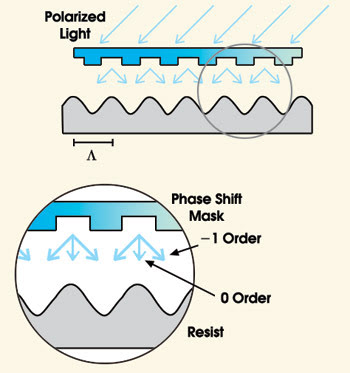
Figure 1. In near-field holography, if parallel (0.1) monochromatic and linear polarized light hits a quartz grating, the zeroth diffraction order will pass through the mask, while the first diffraction order is deflected. Interference between the two beams will result in a specific pattern below the mask that resembles the structure on the phase-shift mask.
The method is called near-field holography because the mercury lamp used as the light source displays only limited coherence. This limits formation of the interference pattern to the field close to the mask. Using a highly coherent laser, the standing waves also would extend into the far field. However, the most economical process for producing fine-pitched gratings would still combine a relatively inexpensive mercury lamp with a small spot size and beam-expansion optics that yield the beam characteristics that are described above.
The master quartz plate (mask) is difficult to make, though, and e-beam writing is not recommended because the limited writing area available in an e-beam writer means that grating lines must be stitched together. This introduces stitching error, which in turn can create undesirable diffraction patterns.
Therefore, it is better to use the crossed-laser-beams technique to form patterns. Once the right pattern has transferred into the quartz plate, the pitch is not susceptible to outside influences and can be replicated from this plate numerous times. (Temperature is well-controlled in a cleanroom, and quartz has a very low coefficient of thermal expansion.)
The near-field holography technique also uses a mask aligner to prepare the substrate to receive the pattern to the master mask. The pattern is then transferred in contact mode. Because no electrical circuits are patterned, occasional line defects caused by the mask contact do not influence the grating efficiency. The resist particles generated are small because of the reduced resist thickness: typically the same as the linewidth (about 100 nm in telecommunications applications).
Manufacturing matters
Jean-Louis A. Roumiguieres and Michel J. Neviere first explored near-field holography as a possible replication method in the early 1980s. Donald M. Tennant from Bell Labs in Murray Hill, N.J., described the first practical manufacturing setup in 1992.1
To work properly, no major reflection of the exposure light from the wafer surface is allowed; otherwise, these rays would interfere with the incoming patterning rays. This is no problem in the case of glass, but it is for highly reflective surfaces like Si or InP. In this case, an antireflection layer must be spun onto the wafer and the photoresist spun on top of the antireflection layer.
The drawback of near-field holography when using a conventional mercury-type lamp is low intensity and the need for good contact between mask and wafer. Only a part of the lamp radiation can be used because of the high collimation requirement and the fact that only one spectral line of the mercury spectrum can be employed. Finally, the polarization requirement kills 50 percent of the available light. However, no large wafer volumes are produced in most applications, so there probably would be no need to change the light source.
Figure 2. This 240-nm grating was produced by a 1-in. mask on a 2-in. wafer. In the image, white light illumination is directed toward the substrate, with diffracted light coming back to the observer.
One key application of this technique is the production of gratings to select a very sharp wavelength from distributed feedback solid-state lasers. These lasers are small, so thousands can be produced on a single InP wafer. In this case, the small wafer diameter — typically 2 in. — also makes it much easier to obtain a rather good contact between mask and wafer.
Not all kinds of grating pitches can be manufactured with this process. There is a link between the exposure wavelength (λ) and the grating pitch (Λ) if only first- and zero-order are to be present:
λ/2 < Λ < 3λ/2
Because of their selective light sensitivity, only 313-, 365- and 415-nm lines can be used with conventional photoresists (Figure 2). The pitch obtainable in practice is limited to values between 200 and about 550 nm (Figure 3).
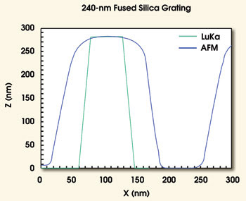
Figure 3. Unlike an atomic force microscope (measurements in blue), an optical diffraction microscope can produce data (green) that allows computer generation of the true line profile of the grating. Grating lines of the sample have a 240-nm pitch.
To observe gratings with pitches produced by near-field holography, it may be necessary to use a specially designed microscope, such as an optical diffraction system developed by Luka OptoScope ApS in Herlev, Denmark. One reason is that a conventional optical microscope may be incapable of visualizing 100-nm lines. A scanning electron microscope requires the destruction of the sample to observe the line cross section. In addition, preparation time is relatively lengthy. An atomic force microscope is limited by the tip radius and cannot display a true cross section of the grating profile.
An optical diffraction microscope, however, makes use of the fact that gratings and the line shape display a unique diffraction pattern when illuminated by a wide continuous light spectrum. A computer can then calculate the true line profile from the values of diffracted light given off by the grating. The measurement is nondestructive, and the profile can be displayed within a minute.
Near-field holography can become an important technique for manufacturing wavelength filters for wavelength division multiplexing and demultiplexing signals in advanced telecommunication fiber networks. The filters are based on accurate distributed feedback laser wavelengths that require manufacturable gratings that display the right pitch. Masks also can be manufactured carrying a variety of grating pitches. Other potential applications are in the areas of biosensors and MEMS.
Reference
1. D.M. Tennant et al (November/December 1992). J. VAC. SCI. TECHNOL.
Meet the author
Elmar Cullmann is a consultant with Suss MicroTec AG in Garching, Germany; e-mail: [email protected].
Key Strengths of Near-Field Holography
1. Complex projection optics such as those used in deep-UV lithography are unnecessary.
2. Defects generated by the contact of the mask and wafer are not as critical as they are in the production of integrated circuits. Despite the contact between mask and wafer, there are no wear-related issues, and the mask can have a nearly unlimited life span. This is key because masks can cost $15,000 or more. Suss MicroTec AG works with ADC Denmark (formerly Ibsen Microstructures) in Copenhagen to fabricate phase-shift masks.
3. Optics adjustments are simple. Only the beam angle must be adjusted with relatively low accuracy. The high collimation and monochromaticity of the light are defined by the optical system, which allows the use of conventional mercury lamps. The mask alone defines the critical pitch required for the target application.