Dave Litwiller, Dalsa Corp.
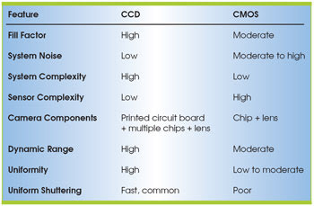
Today, most machine vision systems still rely on some type of CCD imaging sensor, although CMOS devices also are gaining favor. The primary lighting-related differences between these types of sensors are linked to two basic issues: fill factor and the vertical distance the light must travel into the sensor before optical signal sensing takes place.
Fill factor. This parameter defines the portion of each pixel that is optically sensitive. The challenge for CMOS sensors is that each pixel requires a number of transistors and that these transistors are optically insensitive.
CCD technology does not face the same limitation, so fill factors in CCDs for comparable pixel sizes are generally a fair bit better than those in CMOS imagers. Microlens technology can help CMOS sensors compensate to a degree, but because CCDs will retain a fill-factor advantage, they are still more efficient at utilizing incoming light.
Reduction of the fill factor means that fewer of the photons reaching the image sensor generate an electronic signal in the imager. In many applications — both in consumer imaging and in industrial machine vision — systems strain to get enough light, which is lacking because of speed or sensitivity requirements. Engineers call this type of system “light starved.” Throwing away some of the light that is available to the image sensor is a significant issue, given the comparatively high cost of getting more light through brighter illumination systems, larger-numerical-aperture optics or other measures.
Vertical travel distance of light. This is the distance light must travel from the surface of the imager down to the sensing region. The complexity of CMOS imager fabrication means that, in general, there is a taller vertical stack above the signal-sensing region of each pixel than there is in a CCD. The long vertical stack (similar to a pipe to channel the light) means that, compared with a CCD, a CMOS imager has a limited cone of acceptance into each pixel. This not only reduces the amount of light that can be harnessed by the CMOS device, but also causes significant color shifting in color applications.
The shorter the distance the light has to travel, the better the CCDs perform because there are fewer, essentially thinner, layers above the photo site. Thus, the transmission of light from the surface of the image sensor to the signal-sensing region is more robust.
The result is that, when considering lighting issues, CCDs are superior to CMOS devices, both for fill factor and numerical aperture/spectral shift concerns. This holds true for both line- and area-scan cameras, although line-scan technology offers more flexibility as to where transistors can be placed in the CMOS imager. This helps soften the photon-utilization efficiency trade-off compared with CCDs.
Meet the author
Dave Litwiller is vice president of corporate marketing and business development at Dalsa Corp. in Waterloo, Ontario, Canada; e-mail: [email protected].