High-speed camera architectures and multiport CCDs enable the required data rates and dynamic range.
Dr. John R. Tower, Sarnoff Corp.
Fueled by the ever-decreasing size of features on semiconductor wafers, the semiconductor inspection industry continues to focus on shorter-wavelength light (Figure 1). Increasingly, the manufacturers of wafer and reticle (photomask) inspection tools and defect-review imaging technology are developing systems that are based on illumination sources, optics and cameras that operate in the deep-UV, 150 to 300 nm. Wavelengths of interest include 248, 193 and 157 nm (excimer laser wavelengths).
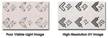
Figure 1. The resolution improvement afforded by imaging at shorter wavelengths is driving more semiconductor manufacturers to use UV imaging during inspection.
The challenge for camera manufacturers is to produce imaging systems that operate at these wavelengths and still transmit data at anywhere from 0.1 to greater than 1.0 gigapixel per second. This emphasis on ever-faster inspection times, driven by the highly competitive nature of the market, will only continue to grow.
High-speed camera systems for these applications usually use either line-scan or staring-area-array architectures. Multiport CCDs tend to be the predominant detector choice because of the required data rates and dynamic range. One high-speed area-array CCD camera from Sarnoff Corp. in Princeton, N.J., uses a 1k 3 1k full-frame, 16-port, back-side-illuminated CCD that operates in the deep-UV with greater than 12 bits of dynamic range at 0.1 gigapixel per second. Technology in development will employ 2k × 2k full-frame CCDs with a data rate exceeding 1.0 gigapixel per second.
Line-scan cameras frequently require a high-speed linear-array CCD. Typical performance parameters might include 7200 × 64 pixels, time-delay and integration, back-side illumination and multiport scanning at 0.4 gigapixel per second (Figure 2). Data rates for next-generation devices will extend beyond 2 gigapixels per second.
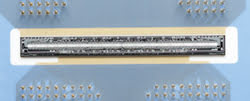
Figure 2. This 7200 × 64 bidirectional time-delay-and-integration CCD provides 0.4 gigapixel per second (8 × 8-μm pixels).
Technology challenges
Deep-UV, high-speed imaging for semiconductor inspection presents some unique challenges related to quantum efficiency, quantum efficiency stability, pixel cosmetics and camera stability. Collectively, these challenges are leading companies to examine new ways of manufacturing high-performance imagers and cameras.
There are two primary methods of achieving useful CCD quantum efficiency in the deep-UV. The first employs a wavelength-converting coating applied to the gate side of the CCD. This coating converts the incident UV photons to visible-light photons that can pass through the detector’s polysilicon gates. The net quantum efficiency of this approach is typically 20 to 30 percent.
The second method, based on thinned back-side-illuminated CCDs, directly converts UV photons into photoelectrons at the back surface of the silicon. The net quantum efficiency depends on the processing and antireflection coating details. A broadband approach provides a net quantum efficiency exceeding 50 percent (Figure 3). For optimized antireflection coatings, efficiency will exceed 90 percent at selected wavelengths.
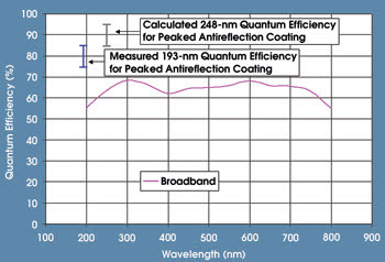
Figure 3. Antireflection coatings can offer quantum efficiency exceeding 90 percent for certain wavelengths. This is illustrated by the UV quantum efficiency of back-side-illuminated CCDs: measured broadband curve, measured 193-nm optimized and projected 248-nm optimized.
A major challenge with any method is to achieve both quantum efficiency stability and very good pixel cosmetics at deep-UV wavelengths. Because of the photons’ high energy, the absorption depth for direct UV imaging is very shallow. At 250 nm, the absorption depth in silicon is 50 Å (within 50 Å, 60 percent of the photons are absorbed). This involves roughly 10 atomic silicon layers. Care must be taken to avoid dead-band or recombination at the first silicon surface of the back-side-illuminated CCD, and to properly treat the surface so that performance will not degrade over time.
Camera design
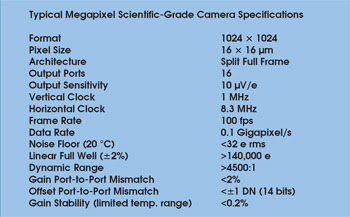
To achieve the high pixel rates with multiport CCDs, two types of cameras for staring arrays have been developed at Sarnoff. The first is a custom design optimized for maximum dynamic range, linearity and stability (see table). One example is a 16-port, 1k × 1k device that outputs data through 16 fiber optic cables. Each pixel is digitized to a depth of 14 bits.
 A second type of multiport camera is built upon a more flexible, expandable architecture, and the data output follows the Camera Link protocol. The same 16-port, 1k × 1k CCD may be run in this camera system (the CAM 1M-100), providing two digital outputs. The eight output ports on the top of the detector are reorganized in the camera and output over one digital channel, with the second digital channel providing the output from the eight ports on its bottom side. Each pixel is digitized to a depth of 12 bits.
Keeping pace
Beyond this, a new generation of CCDs and higher-speed versions of the camera are being developed. One focus of this development is a 2k × 2k full-frame camera capable of 250 fps. Expected performance characteristics will include high sensitivity (quantum efficiency greater than 50 percent), high resolution (13-μm pixels with high modulation transfer function), wide dynamic range (11 to 12 bits), antiblooming and deep-UV imaging at high data rates (gigapixel per second).
The semiconductor inspection industry has demanding needs for deep-UV, high-speed imaging. Back-side-illuminated multiport CCDs and high-performance camera systems are meeting those needs. The imaging technology will continue to advance at a rapid pace, given the fast pace of the advancement of integrated circuit wafer fabrication technology and the competitive need for the next generation of higher-resolution and higher-throughput inspection equipment.
Meet the author
John R. Tower is senior technical director of the Imaging Technology and Products business unit at Sarnoff Corp. in Princeton, N.J.; e-mail: [email protected].