Tom Calahan, Carl Zeiss MicroImaging Inc.
Many materials manufacturing applications today, including coating deposition, semiconductor production, microelectromechanical systems (MEMS) and micromachining, require precision surface step-height measurement. To measure simple surface height structures, many of these applications still use tools such as contact profilometers, atomic force instruments and some interferometer-based systems, which frequently are complex, costly, time-consuming and difficult to set up and align. One solution is a technique that Carl Zeiss MicroImaging Inc. engineers call total interference contrast, which can turn an optical microscope into a microinterferometer.
MEMS topographic characterization is an emerging area that can benefit from a simplified optical analysis and height measurement technique. Many fabrication properties are determined mainly by the thickness of the deposited material. When using techniques such as pulsed laser deposition or etching, engineers must monitor height, thickness and homogeneity, especially when prototyping the process (see figure).
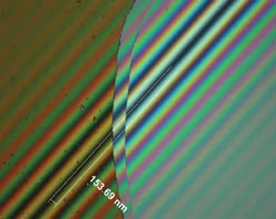
Using a polarization/optical shearing microinterferometer can facilitate optical analysis and height measurement of thin films. This total-interference-contrast reflected-light image of an amorphous ZrO2 coating on a ceramic substrate was taken with a 10× objective.
If the substrate and features are of different-type materials, it is important to understand the material-dependent phase shift in reflected light from the various material types. For example, TiO2 has a phase shift at 136°; ZrO2 at 159°.1
This issue can be critical when depositing materials on glass, where measurement values can be distorted significantly. It also is recommended when transparent layers must be measured on a nontransparent substrate, where issues such as dispersion effects can influence the measurement. In recent tests with a pulsed laser deposition system, the microinterferometer was found to monitor both sets of process parameters with accuracy on a par with atomic force microscopy and contact profilometry.
The total-interference-contrast accessory works with a reflected light microscope to measure surface height topography in the range from 20 nm to 5 μm with a resolution of a few nanometers. As with other contrast techniques, differences in height of the specimen structure are determined by using a camera-based digital imaging system to measure the shift in the interference fringes that are superimposed on the area of interest. The fringe spacing information also can be used to calibrate the imaging system because the distance between fringes is related to one-half the wavelength of light and is typically 275 nm.
The optical principle behind total interference contrast is polarized, reflected-light, optical shearing interferometry, where two images of the sample area are created, shifted a distance apart and recombined to produce interference fringes on the area of interest. This differs from other contrasting techniques in that it uses circularly, instead of linearly, polarized light.
This allows end users to rotate and align the fringe pattern to the imaged structure being measured without altering of the contrast of the interference pattern. There is no need to rotate the microscope stage to optimize the specimen orientation, as is required with conventional polarization interferometers, and this can be useful when a surface has diverse structures in various directions. Using an image shearing technique, the total-interference-contrast device also creates its own reference beam path to alleviate alignment issues often associated with other microinterferometers, such as critical sample leveling and reference beam path matching.
The ability to measure precise step height and layer thickness thus can increase the optical microscope’s measurement and analysis flexibility in surface analysis for R&D, quality control and failure analysis in a variety of industrial applications. Some work still must be done to utilize this technique for more complex feature structures; however, it offers a few distinct advantages, such as simple alignment and setup, noncontact measurement, built-in calibration, operation with all objective magnifications and less sensitivity to vibration than most other similar measurement systems.
Reference
1. Bernd Schey et al (2004). Pulsed laser deposition and TIC microscopy…. PHOTONIK, Vol. 36, No. 3.
Meet the author
Tom Calahan is a product manager of material microscopy with Carl Zeiss MicroImaging Inc. in Thornwood, N.Y.; e-mail: [email protected].