
Building Better LEDs from the Bottom Up
Hank Hogan
An LED manufacturing technique that promises to enable the production of brighter and more efficient devices has been demonstrated by investigators from National Cheng Kung University in T’ai-nan and Wu-Feng Institute of Technology in Chia-i, both in Taiwan. They employ a highly conductive nickel layer for the LED foundation and a laser liftoff process to free the devices from a performance-hindering sapphire substrate.
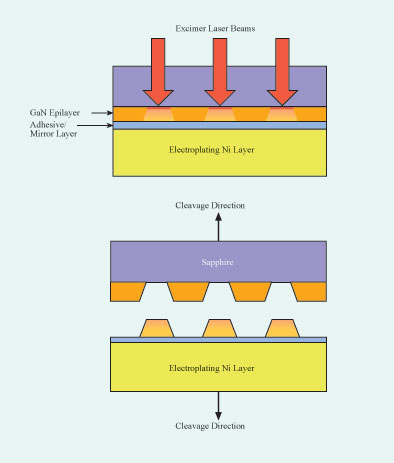
The LED manufacturing process incorporates the addition of an electroplated nickel layer and laser liftoff. The resulting structure has the cathode and anode on opposite sides of the emitter. Courtesy of Shui-Jinn Wang.
The method results in devices with high thermal conductivity, a low current crowding effect, and shorter and higher conductivity of the current conduction path, said Shui-Jinn Wang, an electrical engineering professor at the university. Traditional GaN LEDs are grown on sapphire, which is a poor conductor of heat and electricity. Consequently, both LED contacts, the cathode and anode, must be built on the nonsapphire side of the device. As a result, the current crowds together, lowering overall performance.
The researchers solve this problem by adding a few steps to the standard LED manufacturing sequence. They first coat a GaN epilayer grown atop a sapphire substrate with a 45- to 50-μm-thick electroplated layer of nickel. They use patterned laser lift-off to remove the sapphire, firing 25-ns pulses of 248-nm radiation from a KrF excimer laser through a copper mask placed on the back of the transparent sapphire. The laser causes local heating in the GaN layer, allowing it to lift off in a pattern determined by the mask.
Wang noted that this separation causes mechanical stress, which can produce performance-degrading defects. However, he said that the stress can be reduced by careful mask layout.
In the final fabrication steps, the researchers clean up residue from the separation process and place a contact on the bare side of the GaN layer. The resulting structure has the cathode and anode on opposite sides of the LED, eliminating current crowding and offering other advantages, Wang said.
“Since there is only a single contact pad on the light-emission side of the device, the effective light-emitting area of the new device is larger than that of the regular one of the same chip size.”
In tests of the fabrication technique, the scientists found that the new devices had double the light output of standard LEDs of the same size. They also had lower forward voltage drops, 0.35 and 0.89 V, at injection currents of 20 and 80 mA, respectively.
There is commercial interest in the process, Wang said, with a focus on the production of large-area, high-power LEDs.
Applied Physics Letters, July 4, 2005, 011111.
Published: September 2005