Femtosecond lasers enable microfabrication with resolution beyond the diffraction limit.
Andreas Ostendorf and Boris N. Chichkov, Laser Zentrum Hannover eV
The rapid technical development of ultrashort laser systems is creating exciting possibilities for very precise localization of laser energy in time and space. These achievements have triggered novel laser applications based on nonlinear interaction processes.
A promising three-dimensional microfabrication method that has recently attracted considerable attention is based on two-photon polymerization with ultrashort laser pulses.1-5 When focused into the volume of a photosensitive material (or photoresist), the pulses initiate two-photon polymerization via two-photon absorption and subsequent polymerization. After illumination of the desired structures inside the photoresist volume and subsequent development — e.g., washing out the nonilluminated regions — the polymerized material remains in the prescribed 3-D form. This allows fabrication of any computer-generated 3-D structure by direct laser “recording” into the volume of a photosensitive material (Figure 1).
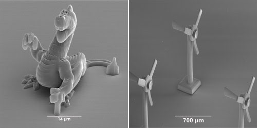
Figure 1. These SEM images show a micro-scale dragon (left) and a movable windmill (right) fabricated by two-photon polymerization in organically modified ceramics.
Because of the threshold behavior and nonlinear nature of the process, a resolution beyond the diffraction limit can be realized by controlling the laser pulse energy and the number of applied pulses. As a result, the technique provides much better structural resolution and quality than the well-known stereolithography method.
Three-dimensional microstructuring of photosensitive materials by two-photon polymerization is effective for the fabrication of 3-D structures having a resolution of 100 nm or better. For two-photon polymerization and 3-D materials processing, computer-controlled positioning systems are combined with a light source that is typically a near-infrared Ti:sapphire femtosecond laser oscillator emitting at ~800 nm.
To benefit from the high resolution inherent in the two-photon polymerization process, highly accurate positioning systems — e.g., piezoelectric stages and/or scanners — are required. However, piezoelectric stages have a traveling range of only a few hundred microns in each direction. Alternatively, optical scanning systems can be used to move the laser beam, but they must deflect the writing laser beam through the outer edges of the focusing optics, which can cause distortions in the outer parts of the image and a subsequent loss of intensity and structural homogeneity.
3-D microstructuring system
To overcome these limitations, Laser Zentrum Hannover eV has developed an autonomous, movable system for the generation of micro- and nanoscale 3-D structures. The system integrates a femtosecond laser, a scanner for fast writing of small-area structures and a motor-driven linear positioning system from Aerotech GmbH that uses air bearings. The laser is a compact Ti:sapphire system from High Q Laser Production GmbH, with 200-mW of average power, an 800-nm wavelength, a pulse duration below 100 fs and a repetition rate of 73 MHz.
The positioning system, with three axes, provided a traveling range of 10 cm in each direction. Now commercially available, the 3-D system is equipped with a rotational axis that allows curved cylindrical structures to be created by two-photon polymerization (Figure 2). 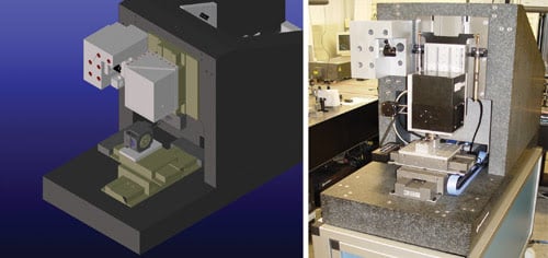
Figure 2. Front view of the 3-D microstructuring system shows a CAD drawing (left) and a photograph (right).
For two-photon polymerization microstructuring, an X-Y galvo scanner deflected the expanded laser beam through the high-numerical-aperture immersion-oil objective, which focused the femtosecond pulses into the photosensitive material, or resin (Figure 3). The scanner was mounted on the Z-axis of the large-range X-Y positioning system. The CCD camera enabled real-time process monitoring. The sample was mounted on a 2-D translational stage.
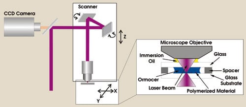
Figure 3. This is the principal setup for 3-D writing and structuring.
By using a scanner and translational stages to move the tiny beam waist three-dimensionally inside the resin, one can write complex 3-D structures. The accuracy of the scanner-based writing is ~100 nm, while the positioning accuracy over the complete travel range is better than 400 nm.
Negative- and positive-tone photoresists are the two types of photosensitive materials that can be structured by two-photon polymerization (Figure 4). With negative-tone photoresists, two-photon exposure results in cross-linking of polymer chains, allowing the unexposed resist to be washed out. With positive-tone resists, light exposure leads to chain scission, creating shorter units that can be dissolved and washed away in the development process. Most hollow structures can be machined by removing only a small fraction of the total material in the original workpiece; in which case, positive-tone photoresists are more efficient.
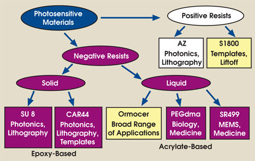
Figure 4. Photosensitive materials are studied at Laser Zentrum Hannover eV.
Negative-tone resist materials can be divided into solid and liquid subgroups. The solid materials shown in Figure 4 are epoxy-based cationic photoresists. In cationic systems (such as the commercially available SU 8 photoresist) an acid is generated upon laser irradiation. In this case, polymerization does not take place during laser irradiation (only after a postexposure bake). This is an important property of cationic photoresists because the difference in the refractive index of exposed and unexposed areas is negligible, which allows for a flexible irradiation strategy and for combining direct laser beam writing with holographic exposure.
Real-time monitoring
Liquid materials, except organically modified ceramics (Ormocers), are acrylate-based, and the polymerization reaction is triggered by radically reacting photoinitiators during laser irradiation. This allows real-time optical monitoring of the polymerization reaction.
We often use inorganic/organic hybrid polymers (Ormocers) from Micro Resist Technology GmbH in our work. They are synthesized by sol-gel processing,6 whereby inorganic units are connected to organic moieties on a molecular level.7 The polymers are hybrids, combining the properties of organic polymers (low-temperature processing, functionality and toughness) with those of glasslike materials (hardness, chemical and thermal stability, and transparency).8 This allows one to achieve material properties not accessible with composite or polymer materials.
Applications in photonics
Because of their unique optical properties, these polymers are effective for the fabrication of micro-optical components and devices such as microprism arrays and diffractive optical elements (Figure 5).
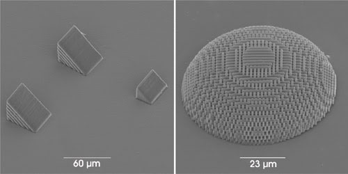
Figure 5. SEM images of micro-optical elements are fabricated by two-photon polymerization.
Further miniaturization of optical elements to the subwavelength size requires new techniques. The use of surface plasmon polaritons on metal surfaces as information carriers in a kind of “optical circuit” is one such method (see “Nanophotonics with Surface Plasmons,” Photonics Spectra, January 2006, p. 56). Surface plasmon polaritons are electromagnetic excitations propagating along and bound to an interface between a metal and a dielectric. They can carry information along metallic waveguides on a dielectric substrate or along dielectric structures on metal surfaces such as bends or splitters (Figure 6). These structures have been fabricated by two-photon polymerization of Ormocers on a gold surface.9
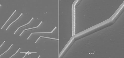
Figure 6. Bends and splitter structures are fabricated by two-photon polymerization on metal surfaces for plasmonic applications.
Two-photon polymerization is rapidly developing as an enabling technology for the fabrication of 3-D photonic crystals and photonic-crystal templates. In particular, it allows the introduction of defects at any location in a substrate, which is crucial for practical applications. Photonic crystals are periodic structures consisting of spatially alternating regions with different dielectric constants.
Propagation of light inside a certain frequency range — the photonic bandgap — is precluded in such structures. If the dielectric constant periodicity occurs in all directions, then the structure is a 3-D photonic crystal. Depending on the topology and dielectric-constant contrast of photonic crystals, their optical properties can be tailored. Since the concept of a 3-D photonic crystal was introduced in 1987 by Eli Yablonovitch10 and Sajeev John,11 photonic crystals have been the subject of intense research. Despite this, fabrication of photonic crystals with a fully 3-D bandgap in the visible range remains a challenge.
To realize photonic crystals with a full photonic bandgap requires 3-D microstructuring of high-refractive-index materials. The most attractive option is to infiltrate fabricated templates with a high-refractive-index material and then remove the template.5 Using most negative-tone photoresists to fabricate templates is rather complicated because the structures fabricated in these materials are stable and not readily soluble. An example of a photonic crystal template fabricated in SU 8 is shown in Figure 7 (above left). In the case of positive-tone photoresists, the polymer is weakened and is usually more soluble in developing solutions. This is advantageous for the fabrication of 3-D templates. In top right photo, a scanning electron microscope image of the photonic crystal template fabricated in Shipley S1813 photoresist is shown. 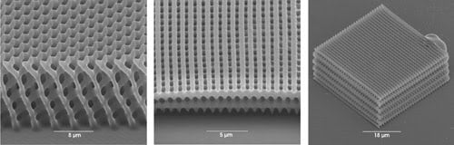
Figure 7. SEM images of photonic crystals are created in SU 8 ( left), S1813 (center) and Ormocers (right).
Another way to fabricate photonic crystals is to use inorganic/organic photosensitive materials with a high degree of inorganic content, as depicted in Figure 7 (left).12 Using this method, it is possible to skip the replication steps and to fabricate 3-D inorganic structures directly. By an appropriate thermal treatment of inorganic/organic hybrid materials, one can remove organic components from the laser-fabricated 3-D structures and leave the purely inorganic part. In this way, the two-photon polymerization technique (or, in general, two-photon-activated processing) and thermal posttreatment can be used to fabricate inorganic 3-D photonic crystal structures.
The two-photon polymerization technique shows promise for biological applications, including tissue engineering, drug delivery, medical implants and medical sensors. For tissue engineering, the ability to produce an arbitrary 3-D scaffold structure is appealing. Scaffolds are required to artificially fabricate living tissue that can integrate with host tissue inside the body, a challenging undertaking. Two-photon polymerization, in combination with the right materials, allows precise control over the 3-D geometry of the scaffold, enabling modeling and reproduction of cellular microenvironments (Figure 8). Furthermore, the high resolution of the technique can provide control over the cell organization inside the scaffold and, consequently, over cell interactions. Another advantage is that the near-IR laser radiation used for two-photon polymerization is not harmful to cells at the applied intensities and also could be used for the manipulation and encapsulation of cells.
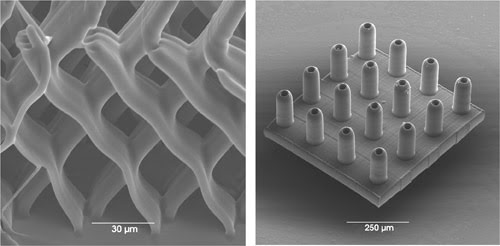
Figure 8. SEM images of scaffold structures (left) and a free-standing Lego-type structure for cell growth experiments (right) are produced by two-photon polymerization of Ormocers.
For applications in biomedicine, Ormocers are interesting materials. Biocompatibility of the polymers has recently been studied, and the results have demonstrated good adherence of cell types to this material and a growth rate comparable to bioactive materials such as extracellular matrix.13
Microneedles
Two-photon polymerization also can be utilized for the fabrication of drug delivery devices; e.g., microneedle arrays.13 These devices enable transdermal delivery of a wide diversity of pharmacologic agents. Application of microneedle arrays may overcome many of the issues associated with conventional intravenous drug administration, including pain to the patient, trauma at the injection site and difficulty in providing sustained release of a pharmacologic agent.
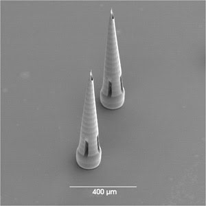
Figure 9. This SEM image shows microneedles for drug delivery fabricated by two-photon polymerization of Ormocers. The microneedles exhibit appropriate mechanical properties and can penetrate skin without fracturing.
Moreover, the flexibility of two-photon polymerization enables arbitrary changes to the needle design and, therefore, comparison of the effect of geometry on mechanical and puncturing properties (Figure 9). Investigations of microneedle arrays for drug delivery are in progress.
Acknowledgment
The authors acknowledge help from Carsten Reinhardt, Sven Passinger and Alexander Ovsianikov of Laser Zentrum Hannover eV in preparing this article, and cooperation from Ruth Houbertz from Fraunhofer Institut für Silicatforschung. They also gratefully acknowledge technical support from Daniel Kopf and Jörg Smolenski of High Q Laser Production GmbH for providing their laser systems for experiments.
Meet the authors
Andreas Ostendorf is executive director of Laser Zentrum Hannover eV, an independent organization carrying out applied research in the field of lasers and optics; e-mail: [email protected].
Boris N. Chichkov is a professor in the department of physics at Leibniz Universität Hannover and head of the nanotechnology department at laser Zentrum Hannover eV; e-mail: [email protected].
References
1. S. Maruo et al (1997). Three-dimensional microfabrication with two-photon-absorbed photopolymerization. OPT LETT, Vol. 22, pp. 132-134.
2. S. Kawata et al (2001). Micromachines can be created with higher resolution using two-photon absorption. NATURE, Vol. 412, p. 697.
3. B.H. Cumpston et al (1999). Two-photon polymerization initiators for three-dimensional optical data storage and microfabrication. NATURE, Vol. 398, pp. 51-54.
4. J. Serbin et al (2003). Femtosecond laser-induced two-photon polymerization of inorganic organic hybrid materials for applications in photonics. OPT LETT, Vol. 28, pp. 301-303.
5. M. Deubel et al (2004). Direct laser writing of three-dimensional photonic-crystal templates for telecommunications. NATURE MATERIALS, Vol. 3, pp. 444-447.
6. C.J. Brinker and W.G. Scherer (1990). Sol-Gel Science. Academic Press, New York.
7. F. Kahlenberg and M. Popall, Mater Res Soc Symp 847, EE14.4.1 (2005).
8. K.-H. Haas (2000). Hybrid inorganic-organic polymers based on organically modified Si-alkoxides, ADV ENG MATER, Vol. 2, pp. 571-582.
9. C. Reinhardt et al (2006). Laser-fabricated dielectric optical components for surface plasmon polaritons. OPT LETT, Vol. 31, pp. 1307-1309.
10. E. Yablonovitch (1987). Inhibited spontaneous emission in solid-state physics and electronics. PHYS REV LETT, Vol. 58, pp. 2059-2062.
11. S. John (1987). Strong localization of photons in certain disordered dielectric superlattices. PHYS REV LETT, Vol. 58, pp. 2486-2489.
12. J. Serbin et al (2004). Fabrication of woodpile structures by two-photon polymerization and investigation of their optical properties. OPT EXPRESS, Vol. 12, pp. 5221-5228.
13. R.J. Narayan et al (2005). Laser processing of advanced bioceramics. ADV ENG MATERIALS, Vol. 7, pp. 1083-1098.