
Patterning Films with Fewer Steps
Hank Hogan
A team of researchers from the University of Illinois at Urbana-Champaign and from Anvik Corp. of Hawthorne, N.Y., has demonstrated a fabrication technique that inscribes patterns onto thin films of indium tin oxide in fewer steps than are typically used in traditional lithography. The group used laser-driven photoablation and subsequent lift-off of an underlying photoresist layer to pattern the material, a transparent conductive oxide used in flat panel displays. Because the new approach has fewer steps, it is potentially faster and cheaper.
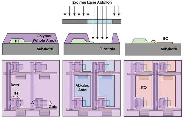
In a novel thin-film patterning process, a resist that covers the entire area (left) is photoablated with an excimer laser (middle). Indium tin oxide is then deposited over everything. When the resist is removed via a lift-off process, the indium tin oxide (ITO)remains where the resist had been photoablated (right). TFT = thin-film transistor. Images courtesy of Kanti Jain, University of Illinois at Urbana-Champaign.
Kanti Jain, a professor of electrical and computer engineering at the university, noted that the technique “can be used in every microelectronic fabrication process, including flat panel displays, micro- and nanoscale semiconductor devices, and flexible electronics.”
In traditional lithography, a photoresist coating is exposed so that a desired pattern is transferred onto it. Subsequent steps involve developing and, possibly, baking the resist to remove it from unwanted areas and to prepare it for further processing, etching the underlying film not covered by the resist and then removing the resist itself.
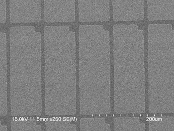
In this scanning electron microscope image, indium tin oxide has been removed in selected spots (darker areas), leaving clean lines and features.
Photoablation, in contrast, requires a single step for patterning because exposure to high-energy photons removes a polymer wherever the fluence is high enough. The technique has been used in a variety of areas, but processing problems including excessive line roughness and high fluence requirements have limited its application. To address these issues, the group turned to the lift-off technique. Here, a polymer film is freed from a substrate; the lift-off removes the film and anything on top of it as well.
In a demonstration of the photoablation and lift-off technique, the investigators deposited a 300-nm-thick layer of Si3N4 atop glass, coated it with a 2.5-μm-thick layer of photoresist and then baked it. They photoablated the resist using projection imaging and a KrF laser from the GSI Group of Novi, Mich., that operated at 248 nm. After the resist was patterned, they sputtered a 60-nm-thick layer of indium tin oxide on everything, then removed the resist via a lift-off process, leaving the film wherever the resist had been removed via photoablation.
Tests with a few dozen repeated pulses and a laser fluence of only 50 mJ/cm2 showed clean patterning of 90 × 270-μm rectangles. The fluence is low enough, Jain noted, that it should be possible to use the technique in flat panel production without harming any thin-film transistors below the indium tin oxide layer. Evaluating the validity of this supposition is the subject of ongoing research.
The technique will be most useful for high-volume manufacturing, where the saving of several steps could have a pronounced effect. The researchers have plans to collaborate with display companies and others to bring the technique into volume commercial application; however, Jain cautioned, this will not necessarily be easy despite the research success. “There are many challenges ahead if it is to be used in mass production.”
Applied Physics Letters, June 25, 2007, Vol. 90, 261102.
Published: September 2007