
A Very Small, Very Cheap Microscope
The device could be used around the world to screen for malaria and other diseases.
Hank Hogan
If manufacturers could mass-produce really small microscopes and sell them for as little as $10, anyone could use them anywhere. A team from California Institute of Technology in Pasadena has devised just such a microscope – one that fits on a single chip yet offers submicron resolution without lenses. The group used this device to image 10-μm-diameter cells and the millimeter-long roundworm Caenorhabditis elegans with a resolution of about 0.8 μm.
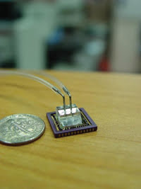
This photograph shows how the small microscope measures up to a dime.
The idea of building a microscope without fancy optics or lenses comes from the floaters in the eye that one sees when looking up at a clear, blue sky. It isn’t that floaters are anything special, noted team leader Changhuei Yang. “They’re debris that has broken off from part of the eye, and they’re just floating around,” he said.
Despite their small size, floaters can be seen quite clearly, even though no lens is involved. The key is that they’re close to the retina, which leads to high resolution.
In the new microscope, the “retina” is a light sensor – a CMOS sensor grid – found in many digital cameras. Similar to the way floaters move by the retina, objects such as cells or C. elegans in the chip, which move by fluid flow, travel past the light sensor. The chip is under constant illumination, so the sensor grid can detect the objects moving past, blocking the light. The Caltech researchers call the device an optofluidic microscope – a combination of optics and fluidics.
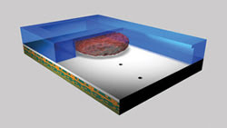
Inside the microscope, objects travel through a fluid channel and pass over holes.
In technical terms, a specimen inside the optofluidic microscope travels across a grid of apertures placed atop a sensor made up of an array of individual pixels. Each aperture acquires an image point of the object. Through raster-scanning in both X and Y, the combination of aperture grid and sensor creates an image of the total object with a resolution equal to the aperture size. The grid density of the aperture array and the pixel size of the sensor are not factors.
The researchers simplified the scanning scheme into a single pass by orienting the grid at a small angle with respect to the object’s flow direction. They also simplified the aperture grid by using a long linear aperture array.
In practice, Yang said, the technique requires that the object not change shape or rotate from one end of the aperture array to the other or the final picture will be blurred. To deal with this possibility, the group came up with a scheme to weed out such errors. They employed two lines of apertures, separated by a suitable distance. Using fluidics, they then forced a specimen to flow past the two lines. By comparing the image generated from one line to the next, they could ensure that the object had not rotated or otherwise changed shape.
Assembling the image from the separate inputs isn’t very hard. “The computation power associated with a PC can probably process 10 of these in parallel,” Yang said.
In building two demonstration devices, the team started with two commercially available CMOS sensors from Micron Technology Inc. of Boise, Idaho. The first had 9.9-μm pixels and the second, 5.2-μm pixels. The researchers planarized the surface of the sensors and coated them with metal. For the first, this was a 300-nm-thick layer of aluminum, while for the second, it was a layer of chromium topped by 300 nm of gold. Then they milled two lines of holes through the metal, placing these so that each mapped to a single pixel. Each line had 100 holes, with the diameter of the holes in the first device a micron and half that of the holes in the second.
Buy the way
Finally, the researchers bonded an optically transparent microfluidic chip atop the sensor, with channel widths of 40 to 50 μm and depths of 13 to 15 μm. The exact depth and width varied according to the application and method of fluid forcing. In all cases, these channels ran across the lines of holes, so that each line crossed the channel at an angle.
To force objects down the channel, they used both a gravity-feed pressure flow approach and one based on electrokinetic drive. They used the former to image the worm C. elegans, achieving results comparable to those with a standard microscope. The images from the demonstration microscope were good enough to distinguish between roundworms with various physical characteristics arising from genetic differences, as reported in the Aug. 5, 2008, issue of PNAS.
Pressure flow can induce rotation in objects, which can hamper significantly the ability of the optofluidic microscope to image round objects. To overcome this, the researchers applied an electric field along the channel, actuating fluid flow by electro-osmosis and helping to lock in the orientation of objects. With this electrokinetic drive technique, the results for 10- to 20-μm-diameter cells, spores and microspheres with the new microscope were comparable to those from a standard one. The data acquisition time was about 0.3 s for a 15-μm object.
During the tests of the optofluidic microscope, roughly half the images were rejected because too much variation was seen between the data acquired from the two lines of apertures. Better flow control and better image processing algorithms could cut that figure, changes that are part of planned improvements.
He noted also keen commercial interest in the device, with some of the possibilities being high parallel microscopes for high-throughput applications like drug discovery. Another possible use for the device would be a shirt-pocket system that could screen for malaria or other diseases in less developed parts of the world.
He believes that a prototype of a mass-produced optofluidic microscope could be available within a couple of years. Commercialization could occur within five years.
Published: September 2008