GAITHERSBURG, Md., April 1, 2009 – A method for engineering the first-ever nanoscale fluidic (nanofluidic) device with complex 3-D surfaces has been realized by researchers at the National Institute of Standards and Technology (NIST) and Cornell University, by way of manufacturing integrated circuits at the nanometer level.
According to the researchers, the Lilliputian chamber is a prototype for future tools with custom-designed surfaces to manipulate and measure different types of nanoparticles in solution.
Among the potential applications for this technology: the processing of nanomaterials for manufacturing; the separation and measuring of complex nanoparticle mixtures for drug delivery, gene therapy and nanoparticle toxicology; and the isolation and confinement of individual DNA strands for scientific study as they are forced to unwind and elongate (DNA typically coils into a ball-like shape in solution) within the shallowest passages of the device.
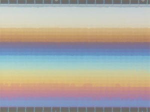
Overhead view of the NIST-Cornell 3-D nanofluidic device showing the different depth levels within the chamber as horizontal bands. The deepest, at the bottom, measures about 620 nanometers (slightly smaller than an average bacterium), while the shallowest, at the top, is about 60 nm (1000 times smaller than the width of a human hair). The colors of the bands result from different mixing of white light components (interference) at each depth. (Images: NIST)
Nanofluidic devices are usually fabricated by etching tiny channels into a glass or silicon wafer with the same lithographic procedures used to manufacture circuit patterns on computer chips. These flat rectangular channels are then topped with a glass cover that is bonded in place. Because of the limitations inherent to conventional nanofabrication processes, almost all nanofluidic devices to date have had simple geometries with only a few depths. This limits their ability to separate mixtures of nanoparticles with different sizes or study the nanoscale behavior of biomolecules (such as DNA) in detail.
To solve the problem, NIST's Samuel Stavis and Michael Gaitan teamed with Cornell's Elizabeth Strychalski to develop a lithographic process to fabricate nanofluidic devices with complex 3-D surfaces. As a demonstration of their method, the researchers constructed a nanofluidic chamber with a "staircase" geometry etched into the floor. The "steps" in this staircase—each level giving the device a progressively increasing depth from 10 nanometers (approximately 6,000 times smaller than the width of a human hair) at the top to 620 nanometers (slightly smaller than an average bacterium) at the bottom—are what give the device its ability to manipulate nanoparticles by size in the same way a coin sorter separates nickels, dimes and quarters.
The NIST-Cornell nanofabrication process utilizes grayscale photolithography to build 3-D nanofluidic devices. Photolithography has been used for decades by the semiconductor industry to harness the power of light to engrave microcircuit patterns onto a chip. Circuit patterns are defined by templates, or photomasks, that permit different amounts of light to activate a photosensitive chemical, or photoresist, sitting atop the chip material, or substrate. 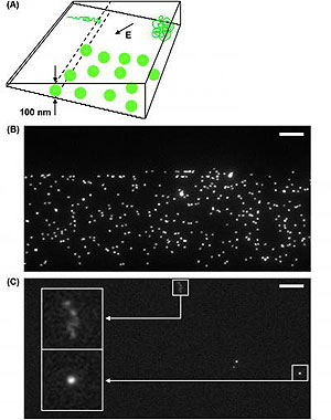
(A) Schematic of the NIST-Cornell nanofluidic device with complex 3-D surfaces. Each "step" of the "staircase" seen on the side marks a different depth within the chamber. The letter "E" shows the direction of the electric field used to move the nanoparticles through the device. The green balls are spheres with diameters of 100 nanometers whose size restricts them from moving into the shallower regions of the chamber. The coil in the deep end of the chamber (upper right corner) is a single DNA strand that elongates (upper left corner) in the shallow end. (B) Photomicrograph showing fluorescently tagged spherical nanoparticles stopped at the 100-nanometer level of the chamber, the depth that corresponds to their diameter. (C) Photomicrograph of a single DNA strand that is coiled in the deep end of chamber (box at far right) and elongated in the shallow end (box at far left). Larger boxes are close-ups showing the fluorescently tagged strands.

The NIST-Cornell nanofabrication process takes advantage of this characteristic, allowing the researchers to transfer a 3-D pattern for nanochannels of numerous depths into a glass substrate with nanometer precision using a single etch.
The result is the "staircase" that gives the 3-D nanofluidic device its versatility.
Size exclusion of nanoparticles and confinement of individual DNA strands in the 3-D nanofluidic device is accomplished using electrophoresis, the method of moving charged particles through a solution by forcing them forward with an applied electric field. In these novel experiments, the NIST-Cornell researchers tested their device with two different solutions: one containing 100-nanometer-diameter polystyrene spheres and the other containing 20-micrometer (millionth of a meter)-length DNA molecules from a virus that infects the common bacterium Escherichia coli. In each experiment, the solution was injected into the deep end of the chamber and then electrophoretically driven across the device from deeper to shallower levels. Both the spheres and DNA strands were tagged with fluorescent dye so that their movements could be tracked with a microscope.
In the trials using rigid nanoparticles, the region of the 3-D nanofluidic device where the channels were less than 100 nanometers in depth stayed free of the particles. In the viral DNA trials, the genetic material appeared as coiled in the deeper channels and elongated in the shallower ones. These results show that the 3-D nanofluidic device successfully excluded rigid nanoparticles based on size and deformed (uncoiled) the flexible DNA strands into distinct shapes at different steps of the staircase.
Currently, the researchers are working to separate and measure mixtures of different-sized nanoparticles and investigate the behavior of DNA captured in a 3-D nanofluidic environment.
In a previous project, the NIST-Cornell researchers used heated air to create nanochannels with curving funnel-shaped entrances in a process they dubbed "nanoglassblowing." Like its new 3-D cousin, the nanoglassblown nanofluidic device facilitates the study of individual DNA strands.
For more information, visit: www.nist.gov