
KNbO3 nanowires generate tunable coherent light for microscopy
A team of researchers from the University of California, Berkeley, and from Lawrence Berkeley National Laboratory, also in California, have employed KNbO3 nanowires as a tunable light source in a novel technique known as scanning light microscopy. The nanowires are nontoxic and stable in physiological environments, making them ideal for a variety of physical and biological applications that could eventually include the characterization of individual cells.
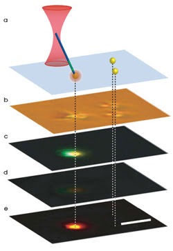
An optically trapped KNbO3 nanowire makes contact with a polystyrene bead (a), shown in a bright-field optical image (b). Color CCD images show both the green light emitted from the nanowire and the fluorescence of the bead (c) and a control image of the beads with no nanowire present (d). The intensity difference between (c) and (d) is obtained by digital subtraction of the red components in each image (e), revealing the orange fluorescence resulting from the excitation by the second-harmonic emission. Reprinted with permission of Nature.
In the experimental microscopy setup, a beam from a 1064-nm continuous-wave infrared laser traps a nanowire between two objectives. The laser functions not only as the trapping wavelength but also as the fundamental beam for visible light generation. When light from the beam enters the end of the nanowire closest to the trapping objective, green light radiates from the distal end of the nanowires.
Because KNbO3, or potassium niobate, is a nonlinear optical material, it reacts to the electric field of high-intensity light — such as that from a laser — in a way that produces new light with a different frequency. One nonlinear process that occurs is second-harmonic generation, in which two photons of the same angular frequency are combined to produce one photon that has twice the frequency, or half the wavelength, of the originals.
Spectral analysis revealed that the emitted light had a wavelength of ~532 nm, a result in good agreement with the theoretically expected value and a demonstration of efficient second-harmonic generation inside the nanowires. Tuning the fundamental input beam over the infrared range will allow the nanowires to generate light across the visible spectrum and to function as a light source for nanowire scanning microscopy.
To see whether the nanowire could be used to image an object, the group scanned the emitted light over a sample pattern made up of gold stripes, spaced by progressively finer separations from 1000 to 200 nm. An Andor Technology high-speed electron-multiplying CCD camera collected the transmitted second-harmonic signal, which was found to decrease when the 532-nm beam passed over each stripe. The spatial resolution of the system depends on the diameter of the nanowire probe; it improves for smaller diameters, but is currently limited to 200 nm.
The nanowires also can be used in fluorescence microscopy, where the distal end makes contact with a 1-mm polystyrene bead containing the fluorescent dye POPO-3. The green second-harmonic wave induces two-photon fluorescence in the bead, which in turn emits orange light at the point of contact with the nanowire. Without the excitation light from the nanowire, the intensity of the orange fluorescence is reduced by a factor of 80.
Researchers Peidong Yang and Jan Liphardt explained that, although they have not yet reported the use of the microscopy technique to characterize living cells, it is something they will pursue after exploring the imaging capabilities of scanning light microscopy with KNbO3 nanowires. They also note that the technique potentially will allow the simultaneous mechanical, optical and chemical characterization of single cells with suitably functionalized nanowires.
Nature, June 28, 2007, pp. 1098-1102.
Published: September 2007