Competition among solar cell manufacturers is rising to new levels as grid parity looms on the horizon. New players are setting up shop for the first time and are implementing state-of-the art production equipment for mass production of high-quality solar cells. Veteran players are expanding and, in some cases, retrofitting existing production lines with newer systems. Not surprisingly, the laser plays a significant role in today’s most advanced solar production systems.
Lasers are used by companies that produce crystalline silicon (c-Si)-based as well as thin-film solar cells. However, lasers are more heavily entrenched in the thin-film technology sector, which is newer, whereas the veteran c-Si manufacturers need proof that retrofitting is worth the investment in time and resources. While thin-film technology currently makes up only about 10 percent of solar manufacturing, traditional c-Si panel makers can benefit from lessons learned in adopting lasers for scribing, patterning, etching and more, from not only the thin-film solar industry but also the display industry. For example, Rofin-Sinar Technologies of Plymouth, Mich., and Manz Automation of Reutlingen, Germany, recently announced manufacturing equipment for the thin-film module industry that includes laser edge ablation and laser cutting. The process stems from Manz Automation’s experience with handling glass substrates for the LCD industry and now combines laser edge ablation and laser cutting for the thin-film solar industry.
Lessons from the thin guys
The thought behind thin film was to develop a method of generating solar power without using expensive silicon wafers. Instead, thin semiconductor layers are deposited on glass, stainless steel or even plastic. The active thin-film layer consists of an absorbing semiconductor. This is sandwiched between two thin-film electrode layers, typically a transparent conductive oxide layer on one side of the absorbing semiconductor, which lets the light enter, and on the other side a second transparent conductive oxide layer and back reflector or a reflective metal contact. Semiconductor junctions are formed either as a p-i-n device or as a heterojunction. To optimize the module voltage and efficiency, the large panels are segmented into a number of narrow cells across the surface. Lasers are used to scribe isolation lines in the front and back contacts of adjacent cells and to scribe the interconnects through the absorber layer between the cells. The laser patterning processes are performed in between the various coating steps so that the cells are connected in series across the module.
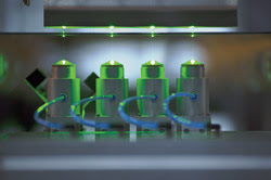
The Oerlikon LSS 1200 is an automated laser processing system that uses multiple beams for high-speed scribing on a thin-film production linePhoto courtesy of Oerlikon Solar.
For thin-film photovoltaic manufacturing, Oerlikon Solar of Truebbach, Switzerland, supplies production equipment and end-to-end production lines that incorporate solid-state lasers for module patterning. According to Heather Booth, head of the laser product group at Oerlikon Solar, “Laser tools are the proven industrial standard, and laser patterning is the de facto method for fine-scribing in thin-film silicon.” The primary reasons that Oerlikon uses lasers in its production lines, Booth explained, are that the devices meet the cost-of-ownership road map and allow for very precise processing. A huge advantage in thin-film processing is “the high throughput that’s achieved whilst maintaining a very narrow scribe region. This minimizes the area that scribes take on the panel, optimizing the module efficiency,” she added.
The lasing advantage
One way that lasers are advantageous in the thin-film process is that coatings can be annealed onto glass without having to be baked in an oven. Instead the coating is applied to the glass, and a laser beam sweeps over it. The glass doesn’t have to go through a cooling process and can be handled soon after the annealing process is complete. Advanced Solar Photonics of Lake Mary, Fla., a solar manufacturer that uses lasers in several areas of its production process, has found that its laser annealing process improves both the efficiency of light transmission and the conductivity of the transparent conductive oxide layers by up to 35 percent.
Short-wavelength green and UV laser solutions commonly have been used for edge isolation in c-Si manufacturing. Now they are starting to be used for scribing trenches, ablating dielectric layers and for drilling through silicon for wrap-through cells. According to Finlay Colville, director of marketing at Santa Clara, Calif.-based Coherent, just as nanosecond UV and green lasers typically were used in the semiconductor and flat panel display industries, now short-wavelength, short-picosecond diode-pumped solid-state lasers are finding a home in both silicon and thin-film solar manufacturing.
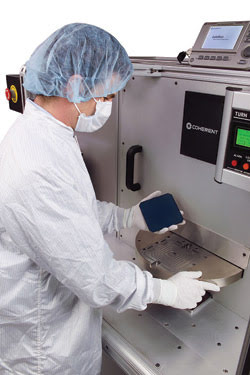
With many laser-based processes being evaluated within R&D or pilot production lines, manual wafer handling is often performed during tool qualification prior to automated production integration. Photo courtesy of Coherent.
Lasers in solar manufacturing are competing with established processes such as plasma etching, screen printing, mechanical cutting and more. In the thin-film industry, Colville said that laser scribing is already a standard because “it’s the only method that can do fine-scribing in a noncontact manner.” Colville acknowledged that the big challenge for laser manufacturers is to show improved return on investment by demonstrating high throughput, better tool uptime, low operating cost, fast wafer processing and more. As the solar road map leads the way to increased efficiency, laser techniques will play an increasingly significant role in both silicon and thin-film solar cell manufacturing.