Dr. Ashok Balakrishnan, Enabelence Technologies, Inc.
The availability of bandwidth-intensive services such as fiber-to-the-home, along with bandwidth requirements in the commercial sector, has created a growing demand for the introduction of new 40G/100G optical networks.
Many new systems rely on advanced modulation formats such as differential phase shift keying and differential quadrature phase shift keying to complement traditional architectures such as dense wavelength division multiplexing. Each method presents substantial optical, mechanical and electronic complexity. Although traditional bulk-optic assemblies can achieve the required complexity in relatively low volumes in some cases, they have considerable problems meeting the additional requirements of volume manufacturability, compactness, ruggedness and low cost.
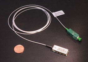
Compact PLC-based transceiver module includes a wavelength division multiplexing filter, a laser, multiple detectors, an amplifier and other subcomponents all integrated onto the PLC chip.
Advanced planar lightwave circuits (PLCs) can achieve the desired level of sophistication in a small, rugged package. These optical chips, similar in many ways to their electronic counterparts, are fabricated using wafer-level processing techniques, and they use optical waveguides to route photons the same way that metal traces are used to route electrons in an electronic chip.
Typical PLC modules for 40G/100G applications require the following subcomponents: a fiber interface, a wavelength filter or combiners, precise phase-delayed optical interferometers, polarization control and polarization-based splitting/combining, optical isolators, laser sources and detectors.
Over the past several decades, PLCs have established themselves as an ideal way to create wavelength filters and stable interferometric structures. They are mass-producible, using the same general techniques as those in the semiconductor industry.
PLC construction
A packaged PLC device consists of a planar chip with passive optical filters and a fiber pigtail. With standard etching and metallization techniques, the planar chip also can serve as a platform for active elements. Recently, successful hybridization methods were introduced onto the PLC platform that efficiently couple lasers and detectors to waveguides using passive automation.
In a bulk optic assembly, lasers are coupled to fibers using one or more bulk-optic lens assembly. In that configuration, changes in mechanical positioning can occur because of temperature drift or stress, which leads to variations of the optical signal. In contrast, lasers can be soldered directly in front of a mode-matched optical waveguide on a PLC. In this configuration, there is little mechanical stress and no distance over which thermal drift can accumulate. Tracking error can be held to less than 0.2 dB quite easily, over a 120 °C range.
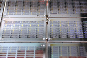
High-volume assembly of planar lightwave circuits (PLCs) includes automated alignment and bonding of lasers, photodetectors and other active components. Photos by Predrag Bosnjak, courtesy of Enablence Technologies Inc.
Optical receivers are fabricated by integrating photodiodes onto the PLC chip itself. In a bulk optic device, a lens is used to focus the incoming light into the narrow aperture of the photodetector. In a PLC, the detector chip can be placed within a few microns of the waveguide carrying the light, enabling the use of narrow-aperture (low capacitance) photodiodes without the need for active alignment.
Between the high-speed photodetector and the external electronics, there is usually a transimpedance amplifier (TIA). The PLC platform allows these TIAs to be mounted onto the optical chip platform, directly adjacent to the photodetector, ensuring optimal signal integrity at high data rates.
Increasing bandwidth
In wavelength division multiplexing systems, data is created as pulses where the signal level is turned on or off to indicate ones and zeros. This method of modulation, sometimes called on/off keying (OOK) suffers from fiber nonlinearity and signal-to-noise problems at high data rates of 40 G per channel. To increase bandwidth, multiple wavelengths are used to pack more signals onto the same optical fiber. In this regime, PLCs have already proved advantageous from a cost and size standpoint, especially for systems with four or more wavelength channels.
To reach higher per-channel bandwidths, sophisticated 40G/100G architectures are being developed that make use of phase-based multiplexing. This is called phase shift keying (PSK).
Differential PSK (DPSK) consists of a single stream of data at a defined bit rate. Through an optical delay line interferometer, data bits are interfered with preceding bits to create an intensity-keyed signal. This interference-based demodulation technique improves signal to noise and, for a variety of reasons, reduces fiber nonlinearity effects.
Because PLCs are manufactured using processes similar to those used in electronic wafers, they afford the possibility of stable delay lines that can be fabricated with photolithographic precision. Polarization effects in the network can be corrected using polarization diversity strategies implemented on the optical chip itself.
Phase shift keying capacity can be increased further using differential quadrature PSK (DQPSK). With this method, information is coded into two quadratures of optical phase, leading to a fourfold increase in the effective data rate. An optical wave can be subdivided into a set of constituent waves that do not mutually interfere.
Although an OOK pulse can represent only two states (0 or 1), a DQPSK pulse can represent four possible states (00, 01, 10 or 11). DQPSK starts with the bandwidth advantages of DPSK, then multiplies the bandwidth by accessing different quadratures (or phases) of light. The optical quadratures must be implemented on the scale of the wavelength of light itself and involve a phase difference equivalent to a few hundred nanometers, which can be extremely difficult to control using anything less than photolithographic precision.
To correctly demodulate a DQPSK signal, two delay lines similar to the ones used in DPSK are needed, but these must be delayed between themselves in phase by only one optical quadrature. This secondary delay must be held to a precision of tens of nanometers. The photolithographic precision of a PLC circuit is ideally suited to DQPSK.
Finally, TIAs, electrical traces (possibly impedance matched), decoupling capacitors and an assortment of small electronic components can be bonded close to the optical circuit – indeed, even immediately above optical waveguides and filters – leading to a high degree of compactness and signal integrity.
Improving functionality
A typical hybrid PLC device consists of small optoelectronic chips and subcomponents integrated onto a larger optical chip, which typically comprises the optical filtering elements and other passive structures. This hybridized subassembly is then placed in a planar package, wire-bonded, pigtailed, lidded and tested for final use.
All of the processes involved in the manufacturing of such a component, from optical fabrication to final assembly, are suited to automated bonding and testing methods. The semiconductor and electronic chip industries have developed pick-and-place and flip-chip bonding processes that are well suited to PLC manufacturing. Wire bonding and postpackaging can be carried over from the electronics industry with little modification.
As customers demand more bandwidth, volume requirements will increase. And as is often the case, costs will continue to decrease despite the added functionality. Meanwhile, with so much deployment under way, ruggedness and reliability become mandatory requirements for any optical component.
Increasing system functionality imposes size restrictions on all components, but collapsing that functionality onto a single integrated optical chip presents an opportunity for meeting the needs of new 40G/100G systems, both now and as their requirements continue to evolve.
Hybrid PLCs represent an ideal choice for low-cost, rugged, compact optoelectronic components for a high-volume market.
Meet the author
Dr. Ashok Balakrishnan is director of product development at Enablence Technologies Inc. in Ottawa; e-mail: [email protected].