Spherical Optics
By Lynn M. Savage, Features Editor
Individually, micro-optics are a few millimeters in diameter at best, but together these tiny lenses comprise a powerful link to future technologies that will affect everything from advanced computers to human health.
Micro-optics permit the manipulation and management of light at a scale that allows photonic systems to more easily connect with electronics, which will help promote optoelectronic communication at faster speeds than have yet been achieved. They are an important technology for the development of improved laser beam shaping devices and optical fiber couplings, for example, and advanced micro-optics support vanishingly small endoscopy devices that help visualize diseases.
Arrays of microlenses make possible unique illumination systems as well as Shack-Hartmann wavefront sensors at the heart of optical coherence tomography systems and the adaptive optics technology that provide twinkle-free astronomy using ground-based telescopes. Micro-optics technologies also have led to the ability to manufacture tiny sensors directly on semiconductor wafers, leading to inexpensive cameras in every cell phone.
One of the key makers of micro-optics and related components is SUSS MicroOptics in Neuchâtel, Switzerland. The company sells micro-optics and related components to more than 200 companies in the semiconductor, laser, sensor, telecommunications, medical and metrology industries and is the preferred supplier for Carl Zeiss SMT GmbH in Oberkochen, Germany.
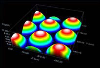
Microlens arrays are used for imaging, metrology and other sensor systems. (Images: SUSS MicroOptics SA)
“Today, micro-optics is key enabling technology for many applications, e.g., deep-UV photolithography equipment used in semiconductor front-end processing,” said Reinhard Voelkel, the company’s CEO. “For deep-UV applications using fused-silica (SiO2) micro-optics, you have to deal with long-term material degradation (compaction) — and for high-power laser, immediate destruction – if light is focused in the bulk material.”
SUSS MicroOptics specializes in manufacturing 8-in.-diameter wafers, from which a multitude of products are made. It also makes refractive spherical and aspherical microlenses, as well as hybrid optics in that scale.
“Our 8-in. wafer technology is based on well-established processes from the semiconductor industry,” Voelkel said. “(The) same cost models apply for our technology: Small series remain expensive; for larger volumes, the prices drop dramatically.”
High-quality CMOS image sensors for cameras, he added, are incredibly cheap if they are manufactured on a very large scale. However, customized CMOS wafers with an atypical design cost a lot more.
As with any other industry, there are challenges ahead for micro-optics manufacturers and end users. Quality and reliability of the optical components are important, especially for integration into machines and manufacturing equipment, Voelkel said, but for areas such as consumer products, like wafer-level cameras and fiber couplers for telecom companies, cost “is everything.”

On wafers up to 8 in. in diameter, intricate diffractive optical elements are possible, including this Fresnel design for shaping the beam of an excimer laser.
While commercial enterprises like SUSS MicroOptics sort out cost issues, basic research remains the domain of academic institutions. Some of these, however, are struggling to settle into a micro-optical niche.
In Europe, for example, the Network of Excellence on Micro-Optics, or NEMO, was started in 2004 with the aim of providing the continent with a complete micro-optical support structure. Funded at €6.4 million, the organization initiated several technology and service centers for the purpose of providing optical modeling, prototyping, integration and packaging services to all of its members and to help set up new standards as necessary.
The organization also set out to direct several application-driven micro-optics topics, including mid-IR optics, subwavelength structured optical surfaces, and nonconventional micro-optical elements. Member groups, such as the Fraunhofer Institute for Applied Optics and Precision Engineering, still excel in micro-optics research, but the group has not been active itself since its original four-year funding expired in 2008.
Similarly, in 2002, researchers and business experts at Clemson University, Western Carolina University and the University of North Carolina at Charlotte (UNCC) started the Carolina Micro-Optics Triangle (CMOT). As with NEMO, the group’s purpose is to join the available research, education and business development resources into a unified force.
Initiated with $31 million, CMOT was to support the creation of more technical jobs in the region, counteracting deep job losses that were occurring in local industries such as textile and furniture manufacturing and tobacco farming. The organization capitalizes on Clemson’s strengths in engineering and advanced materials, UNCC’s expertise in optoelectronics, and Western Carolina’s fast-prototyping capabilities, including injection molding, instrumentation and robotics. Early successes of CMOT presaged the beginning of the Carolinas Photonics Consortium in 2006.
CMOT offers local companies assistance with developing and using advanced technologies, such as providing training on lasers and other optical systems. In all, the group wishes to boost the economic development of the entire region, focusing on existing local enterprises based on automotive and general manufacturing, defense and homeland security, life sciences and telecommunications.
Despite technological strides, the economic situation hasn’t been kind to the group.
“The Carolinas MicroOptics Triangle has been rather quiet lately, in part because we lost support for the person who was helping to coordinate events,” said Mike Fiddy of UNCC, the group’s previous director. Fiddy retired as director in 2010, with Eric Johnson, also of UNCC, taking over.
“Individuals amongst the three universities are still collaborating on research topics, but there have not been any formal events for quite some time,” he said.
Despite moribund funding, however, exciting research continues apace. Fiddy is turning his attention to the optical qualities of metamaterials, for example, while Johnson’s focus is on micro-optics fabrication techniques. A recent resurgence in telecom demand looks to bring back the micro-optical portion of that industry, and the continued drive toward cost savings on wafer-based manufacturing seems certain to push companies to develop new materials and techniques with which to work them into shape.
Lynn Savage
Features Editor