BERKELEY, Calif., Nov. 2, 2011 — Delving into the extreme ultraviolet wavelengths further than ever, a novel microscope is set to provide leaps forward in photolithography technology. The device, dubbed SHARP (for “Semiconductor High-NA Actinic Reticle Review Project”), will have higher resolution, speed, illumination uniformity and coherence control than existing instruments, and is designed to push research toward semiconductors with features as small as 6 nm.
The $4.1 million, 1½-year-long project to build the instrument is a collaboration between scientists at Lawrence Berkeley National Laboratory and leading semiconductor manufacturers. It will be led by Kenneth Goldberg of the Center for X-Ray Optics (CXRO) in Berkeley Lab’s Materials Science Div. Initially, the instrument will be built in parallel with operations at the existing microscope on beamline 11.3.2 of Berkeley Lab’s Advanced Light Source (ALS). By the last quarter of 2012, the new extreme ultraviolet (EUV) photomask-imaging microscope will replace that aging microscope.
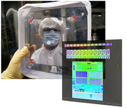
Kenneth Goldberg is seen in the reflective coating of a photolithography mask that he is about to measure at the Advanced Light Source’s 11.3.2 beamline. Inset at lower right shows a mask’s extreme-ultraviolet (EUV) absorbing layer, printed on a 6-in.2 glass coated with multiple layers of molybdenum and silicon to reflect unwanted EUV. The patterned layer represents one level of a working microprocessor or memory chip, which may have 20 or more such levels. (Photos: Lawrence Berkeley National Laboratory)
“EUV light is tricky to work with because every material absorbs it so strongly,” Goldberg said. “So, instead of glass lenses, EUV optical systems rely mainly on specialized mirrors with atomic-scale smoothness, topped by multilayer coatings for high reflectivity.” To maintain efficiency, the entire optical system must be placed in a high-vacuum environment.
The 8-year-old microscope at beamline 11.3.2, dubbed the AIT (for Actinic Inspection Tool), has unique imaging capabilities, but the fast-moving nature of semiconductor technology means that its future is limited. With its higher performance specifications, SHARP should exceed the AIT’s performance and enable forward-looking research years before commercial tools become available.
Within a few years, semiconductor devices used in a wide variety of ever-shrinking electronic devices will be mass-produced in dimensions of 16, 11 or 8 nm.
"As a scientist, I’m excited to contribute something valuable to that ongoing process through my work in extreme ultraviolet photolithography," Goldberg said. "EUV -- using 13.5-nm-wavelength light -- is the successor to today’s deep-ultraviolet lithography (193 nm). It is expected to come into production within the next few years."
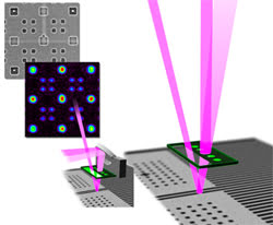
At top left are programmed pattern defects, including the large protrusion in the center, developed by a team at IBM to evaluate printing sensitivity. An image created with the Actinic Inspection Tool (AIT) of the defects is shown at center left. The final stage of the AIT’s beam path is shown bottom left: The synchrotron’s EUV beam enters from the top, reflects from the mask, is focused by an array of zone plates and then reflects from a turning mirror to an EUV-sensitive camera (not shown) to the left. The more efficient SHARP beam path at right removes the turning mirror and a window from the array of zone plates to increase brightness.
But no process is perfect. "Mask defects are a major concern," Goldberg said. "A defect caused by a stray particle on the surface, an unexpected kink in the master pattern, or subtle imperfections in the underlying substrate, can short-circuit a chip or ruin a whole batch."
Other high-resolution tools such as electron microscopes cannot detect the EUV wavelength-specific response of mask patterns and defects, he added. "And that’s necessary to make successful repairs."
SHARP is called an “actinic” microscope because it uses the same EUV wavelengths used in production. Thus, the new EUV microscope will enable semiconductor company researchers to better evaluate defects and repair strategies, mask materials and architectures, and advanced pattern features.
A special feature of the new microscope will be illumination coherence control. The ALS produces an EUV beam with laserlike coherence, ideal for many experiments. For microscopy, however, the image resolution can be improved by a factor of two by carefully re-engineering the illumination into a state called partial coherence. Microscopists have recognized the importance of partial coherence for years, and the synchrotron community is now catching up.
An angle-scanning mirror in the new microscope’s beamline illuminator will take the highly coherent ALS light and steer it into patterns, like a mini-laser-light show, breaking and reshaping the coherence properties. In this way, the SHARP microscope will replicate the properties of current and future tools for lithography production and research, giving researchers the most advanced look at what’s to come.
"With an ability to study defects once considered too small to detect, SHARP will answer pressing research questions about mask defect printability and repair, mask architecture, materials, contamination and cleaning, and more," Goldberg said. "It will be ready at the end of 2012, several years ahead of commercial mask-imaging tools."
For more information, visit: www.lbl.gov