Florent Thibault, Teem Photonics
In a world where the micron has become the standard and competition is fiercer than ever, subnanosecond lasers may be just the answer for emerging industrial microprocessing applications.
Femtosecond and picosecond laser sources, which have been studied extensively over the past 10 years in the academic arena, are considered among the most promising tools for the future. Their exceptional optical performance has been demonstrated over a very broad range of applications, showing the superior quality achieved by ultrashort pulses.
The oscillator architecture – semiconductor saturable absorber mirror or mode locker crystals, dispersion compensation systems, extended optical cavities – typically provides megahertz-level repetition-rate output and nanojoule-level pulses under mode-locking conditions. While those natural operating parameters do not generally fit materials processing requirements, the addition of a regenerative amplification system, pulse picking or sometimes both allows reaching more adequate operating conditions of hundreds of kilohertz or tens of microjoules. These necessary add-ons increase even further the system’s overall performance – and complexity.
Unfortunately, this complexity has a cost impact: an obvious economic cost on one side, and an even more fundamental reliability cost on the other.
Simplicity is bliss
Meanwhile, passively Q-switched microchip lasers feature the simplest existing architecture able to generate ultrashort pulses (Figure 1).
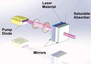
Figure 1. Passively Q-switched laser optical architecture: telecom-grade pump diode, coupling optics and the monolithic microchip cavity (from left to right). Courtesy of Teem Photonics.
Their monolithic laser cavity is made of a double-sliced sandwich of gain medium (Nd:YAG) and saturable absorber (Cr:YAG), with dielectric mirrors deposited on the outer faces. This few cubic millimeter device – embedded in a matchbox-volume package – “naturally” turns the CW pump power provided by a telecom-grade diode laser into a stream of high-peak-power subnanosecond pulses. No need for cumbersome high-voltage controllers or even a water cooling system.
Passively Q-switched microchip technology for industrial lasers covers the range of hundreds of picoseconds down to 300 ps in the offerings of Teem Photonics. Peak powers in excess of 200 kW are readily available at 1 kHz using PowerChip microchip cavities, and a 50-kHz repetition rate and >5-W output power are achievable with the PicoSpark amplified product line.
Unlike other laser technologies, the microchip cavity design fixes the optical pulse characteristics. Pulse energy, width and shape are constant and independent of the repetition rate or output power level.1
Another striking feature of the passively Q-switched microchip technology is its intrinsic ability to generate a high-quality TEM00 diffraction-limited beam. This is due both to the short length of the cavity (and the corresponding Fresnel number of the resonator2) and some soft aperturing effect occurring in the saturable absorber during pulse emission. This excellent beam quality can be conserved during high-power fiber amplification by carefully managing beam properties along propagation.
Last but not least, subnanosecond microchip lasers are by nature fitted to industrial uses and environments, offering a cost-effective, rugged and highly reliable solution.
IR systems operating in free-running conditions reach several tens of million hours’ mean time to failure, while lifetime test lasers are still running with barely no change after more than 50,000 hours (almost six years of 24/7 operation). This is the clear demonstration of what everybody feels: The fewer parts inside a system, the less likely it is to fail.
Hermetically sealed and rugged packaging is an extra guarantee of safe operation in the harshest and most remote environments and prevents extra failures or performance degradation in locations where maintenance must be reduced to the minimum. Some systems currently operate daily in hot and humid conditions in tropical latitudes, in steelworks within highly perturbed electromagnetic environments, or down the pipeline of oil refineries with the same minimum need for maintenance.
The global picture is the same for the green (532 nm), UV (355 nm) and deep-UV (266 nm) offerings. High peak power and beam quality are the two keys for an efficient external-cavity frequency conversion. Then extended lifetime is only a matter of design and know-how. At 266 nm, single-spot lifetime over 25,000 hours has been demonstrated while using some proprietary specific integration processes.
Toward higher power, easier integration
When looking for higher output power, master oscillator fiber amplified-type architecture seems to be an obvious choice. First, it makes the most of the mastered passively Q-switched microchip technology, using it as a seeder. Then a simple amplifier architecture helps keep fundamental problems (reliability, lifetime, manufacturability) under control.
On the technical side, the exceptional subnanosecond pulse characteristics can be preserved and raised to multiwatt levels to meet manufacturing industry requirements. The nanosecond range is a favored temporal zone where nonlinear effects (stimulated Brillouin scattering, self-phase modulation) are low enough not to harm the amplification process.3
The design scheme is straightforward: no need to chirp, stretch or compress pulses, just an efficient single-pass, double-clad fiber amplification stage.
Introducing the amplification stage also enabled the addition of user-oriented functionalities and controls. Real-time pulse energy control and submillisecond start/stop sequences make process definition or automation easier. Synchronization outputs or triggering electronics provide time control for optical pulse emission. Finally, interlock signal management or user available laser status outputs will ensure safe integration into the
production environment.
Materials processing with ultrashort pulses
It is well-known that femtosecond and picosecond lasers can provide a real “cold” materials processing capability. Coupled with a thorough process optimization, that capability leads to the most extreme processing quality. But important questions remain: Is this ultimate level of quality really needed by the market itself? In cases where it could be a technical advantage, is it economically sustainable?
From an industrial point of view, the answer is clearly negative for numerous micromachining applications. Depending upon the strategic market, the global production cost figure or simply the economic environment, the implementation of such a cutting-edge tool may not be affordable or even worth it.
Subnanosecond lasers offer a ready-to-use industrial solution to bridge the gap between the needs for improved
processing quality and decreased cost.
For industrial applications, the sub-nanosecond range brings a pulse width reduction of 10 to 100 times compared with established nanosecond-pulse technologies, with the corresponding large benefits in terms of processing quality. The pricing is similar to that for actively Q-switched or fiber lasers, and the cost of ownership is close to nothing.
Furthermore, decreasing pulse width often goes along with higher processing efficiency – e.g., lower output power need – in a number of cases (brass, copper, molybdenum, nickel, stainless steel),4 decreasing the manufacturing cost even further.
For emerging applications focusing on processing quality, subnanosecond lasers are obviously competitive with ultrafast lasers, with a price per watt that is five times lower. Furthermore, there is no extra investment because they can operate with established beam-steering and beam-shaping technologies. Their processing efficiency is higher in a number of materials, such as silicon or aluminum, where the residual thermal part in the laser-matter interaction actually enhances the ablation process.4
For all cases considered, air cooling avoids the cumbersome need for water management. Compact packaging makes integration easier. Highly efficient lasers coupled with efficient electronics will reduce the power consumption bill or enable new mobile applications.
Materials processing applications
One thing is for sure: Passively Q-switched lasers are not the most effective choice for cutting a 1-cm-thick stainless steel plate. Due to their short-pulse nature and typical high repetition rate (up to 140 kHz), they are well suited for high-quality submillimeter-scale processing – in essence, all kinds of micromachining applications, such as selective ablation, scribing, texturing and fine cutting.
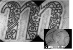
Figure 2. High-speed BK7 glass surface scribing with a 532-nm PicoSpark: no microcracking, 10-µm linewidth and micron-scale chipping. Courtesy of Musée de la Dentelle in Retournac, France.
The type of processed material doesn’t really matter. As with ultrafast lasers, subnanosecond laser-matter interaction occurs in a vaporization regime, where the nature of the material is not a predominant factor compared with thermal regimes. You can definitively process ceramics, diamond, glass, silicon carbide or tungsten with the same laser. Figure 2 shows glass surface scribing without any microcracking, a 10-µm linewidth and micron-scale chipping.
Hard-materials processing quality is illustrated in Figure 3, where a 400-µm-deep rectangle has been machined in a polycrystalline diamond tool. The processed surface roughness is Ra = 6 µm, similar to the unprocessed material. The edges are sharp and well-defined; the walls are nearly vertical with only a 10° slope; and there is no sign of carbonization. Similar processing quality has already been demonstrated in natural tooth, alumina ceramics and silicon.
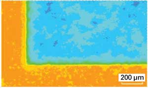
Figure 3. Laser scanning confocal microscope close-up of a synthetic diamond tool machined with a 532-nm PicoSpark: sharp and regular edges, steep flanks and a fairly flat processed bottom surface. Courtesy of Fraunhofer-ILT, Aachen, Germany.
Ultraviolet-amplified passively Q-switched lasers are also particularly successful at processing transparent materials. UV PicoFlash has been introduced recently for eye surgery, as it can make the flaps needed for lasik with quality similar to that produced by the currently used femtosecond technology (Figure 4). They are also able to cut or drill transparent polymers like PET (Figure 5) or polyimide Flex-PCB without any visible heat effects.
Micron-scale 3-D resolution can be routinely achieved with subnanosecond laser processing. TEM00-grade Gaussian beam quality and the availability of deep-UV wavelengths ensure tight focusing. And the reduced energy level for processing and the shorter heat diffusion time minimize heat penetration into the lattice.
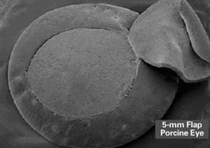
Figure 4. Porcine eye cornea-cutting demonstration with UV PicoFlash. Courtesy of BMO, Lübeck University, Germany.
Confining the interaction volume is indeed of crucial interest for selective ablation processes (selective removal of submicron thin films, laser liftoff) or high-density surface patterning. The 532-nm PicoSpark has been successfully used for P2 and P3 thin-film solar cell manufacturing processes, and for motor engine metal part texturing. Similarly, the 266-nm PowerChip can be used for submicron patterning of metal injection molds, providing a drastic maintenance cost reduction compared with excimer lasers.
Beyond materials processing
Subnanosecond lasers also see growth from more established segments, coming notably from the improved UV and higher power that products offer.
The most promising sensing applications are without a doubt photoluminescence-based materials composition analysis (UV LED, AlGaN-HEMT wafer) and gas sensing for civil or defense applications.
Another strong potential application lies in transparent media marking for traceability or anticounterfeit uses, where the lasers have demonstrated controlled and repeatable semi-invisible bulk marking in a variety of materials.
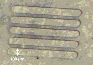
Figure 5. 100-µm-width slits cut in 15-µm-thick PET sample with a 355-nm PowerChip: no visible burrs, melted debris or carbonization on the edges (Note: The structure on the background comes from the holding tissue frame). Courtesy of Fraunhofer-ILT, Aachen, Germany.
Meet the author
Florent Thibault is the support and development manager for new accounts at Teem Photonics in Meylan, France; email: [email protected].
References
1. J.J. Zayhowski (Sept. 27, 1999). Microchip lasers. Opt Mat, pp. 255-267.
2. A.E. Siegman (1986). Lasers. University Science Books, Mill Valley, Calif.
3. P.E. Schrader et al (Nov. 27, 2006). High-power fiber amplifier with widely tunable repetition rate, fixed pulse duration, and multiple output wavelengths. Opt Exp, pp. 11528-11538.
4. J. Lopez et al (2011). Comparison of picosecond and femtosecond laser ablation for surface engraving of metals and semiconductors. Key Eng Mat, Vol. 496, pp. 61-66.