
Ultrafast Lasers Enable Improvements in Microprocessing
Tim Gerke, Fianium Inc.
Ultrafast lasers provide an avenue into a number of new microprocessing applications because of their capability for athermal ablation and their extremely high peak power. Many materials and applications can be susceptible to adverse heating effects such as melting, peeling, chipping, melt splatter and substrate damage when processed with CW and long-pulse lasers. With picosecond and femtosecond lasers, however, these undesirable side effects can be mitigated or eliminated completely. In addition to decreasing heating effects, using ultrashort pulse widths can increase process efficiency and even enable new applications – such as internal marking or scribing of bulk transparent materials – that otherwise are impossible with CW or longer-pulse-width lasers.
These benefits can be demonstrated using an array of high-energy fiber lasers with pulse widths of 2 to 400 ps and pulse energy up to 125 μJ. The lasers used in the demonstrations discussed here are installed in an applications lab in Portland, Ore., on 2-D galvanometer scanner-based processing systems, as well as in a fixed-focal-spot station used for creating very small laser spot sizes. Both processing systems are computer controlled and synchronized with the laser system for full control and arbitrary pattern processing.
This article discusses, by way of particular representative examples, the advantages of ultrafast lasers over longer-pulse lasers for microprocessing applications. Actual commercial use may require the licensing of intellectual property, depending on details of the application, the system assembled or the particular method practiced.
Athermal, high-quality processing
Many microprocessing applications can be executed with nanosecond lasers – but with a significant loss in the quality of the result. Such lasers fundamentally impart much more heat to the material and result in melting, cracking, surface composition changes and other detrimental side effects. With ultrafast laser machining, however, truly athermal processing can be achieved on any material and in any application. One particularly good match for high-energy picosecond lasers is thin-film processing. In this application space, lasers with very moderate pulse energy have been shown to be capable of high-speed material removal with excellent qualitative results, while nanosecond lasers often struggle to achieve equivalent quality and are prone to a number of defects. The heating of thin-film parts due to the long nanosecond pulses can cause an array of detrimental side effects from recast lips, melting, chipping, or substrate cracking or damage.
Figure 1 demonstrates one such defect that can occur in thin-film microprocessing with nanosecond lasers. In the figure, a thin film of molybdenum on a thick glass substrate was laser-scribed with singular pulses in a back-side (superstrate) geometry, where pulses are focused through the glass substrate onto the back of the film. The film is then removed in a liftoff process. In the 10-ns case (Figure 1c), small bits of material are peeling off around the edges and protruding vertically from the film surface, and one such example can be seen on the left edge of the scribe just below center. For conductive materials, this sort of defect is often catastrophic for device functionality.
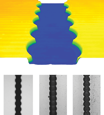
Figure 1. Scribes of thin metal film on glass using (a) 415-ps, (b) 46-ps, (c) 10-ns and (d) 100-ns pulses.
For the 100-ns case (Figure 1d), a lot of material has been deposited onto the surface in the form of splatter, which can result in shunting across the scribe, rendering it useless for electrical isolation applications. In addition to the chipping and melt-related defects from the processed film, the relatively high laser energy resulted also in microcracking of the underlying glass substrate, which can be an impediment to applications where the structural integrity of the substrate is of concern. Overall, there are significant issues with the results achieved from processing this thin metal film with nanosecond systems.
On the same material, we also investigated the results of picosecond pulse widths from 4 to 415 ps using Fianium laser systems, and the picosecond results were qualitatively far superior to the nanosecond results. No modification to the substrate was observed, and no film chipping, cracking or melting was apparent. Processing debris was also not observed. Figures 1a and 1b show the results of 415- and 46-ps pulse widths, respectively. Both results demonstrate typical high-quality, fully isolating scribes of the thin-film material using single laser pulses. Such results are achievable even up to well over 1 m/s with relatively low power (<2 W) lasers or over 10 m/s with higher-power lasers such as Fianium’s Hylase system (8-25 W).
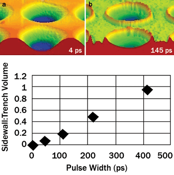
Figure 2. 3-D surface profile images of bulk steel surface textured by multiple pulses per dimple using 4- and 415-ps laser systems (top). A plot of the sidewall:trench volume ratio as a function of pulse width (bottom).
Improvements from ultrafast laser solutions are not limited to thin-film applications, however. Applications involving microprocessing bulk materials, such as metals and semiconductors, can also significantly benefit from ultrafast laser sources. For short (<20 ps) pulses, many of these materials can be machined athermally with no melting. With longer-pulse lasers, even still within the picosecond regime, the thermal effects can become apparent. Figure 2 demonstrates that, even with subnanosecond pulses, melting occurs and results in a recast lip on a laser-surface-textured bulk steel part. When the identical process is run with shorter 4-ps pulses, however, no recast is observed, and more material is removed to form deeper dimples.
The plot at the bottom of Figure 2 demonstrates the trend of the volume of material in the recast sidewall, relative to the removed volume. At 4 ps, where there is no sidewall, the ratio is zero. As the pulse width increases to 415 ps, the ratio increases to nearly unity, where the volume of material removed is approximately equal to the sidewall volume. At this value, the material in the trench is not actually being removed from the substrate; instead, it is simply being pushed to the side.
Increase in efficiency
In addition to avoiding heat-related defects, ultrashort pulse widths can improve processing results through increased efficiency. The long interaction time associated with nanosecond- and longer-pulse lasers results in more energy being wasted, because heat results in melting and can also quickly diffuse out of the modification area. Ultrashort pulses, on the other hand, have such short interaction times that virtually all of the energy applied by the laser pulses is directly utilized in the ablation mechanism and results in a more efficient process.
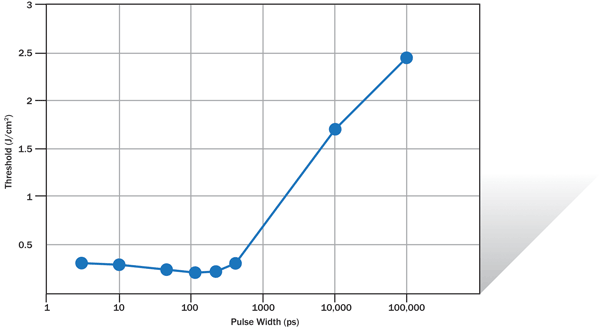
Figure 3. Plot of threshold for thin-film removal vs. pulse width. The removal threshold is flat for the picosecond regime and increases dramatically into the nanosecond regime.
One example of this trend: The laser energy required to scribe or pattern thin films on bulk substrates increases with pulse width. This type of application is often utilized in a liftoff or superstrate processing geometry, where the laser energy is absorbed in the film-substrate interfacial region. Some small fraction of the film is vaporized, and the resulting vapor pressure trapped between substrate and film ejects the film within the processing area.
The plot of experimentally measured thin-film removal threshold versus pulse width (Figure 3) demonstrates that, in the picosecond regime, the removal threshold of thin molybdenum films is around 0.25 J/cm2. When the pulse length increases into the nanosecond regime, the removal threshold increases significantly, requiring an order of magnitude more pulse energy than the picosecond case for the same removal area.
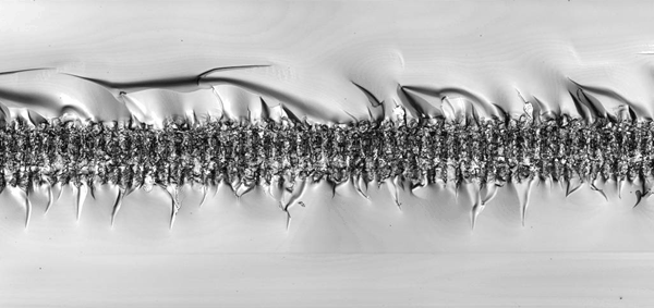
Figure 4. Break edge of a sapphire wafer that has been scribed internally.
This trend demonstrates that a 10- to 100-ns laser would need to have approximately 10 times more pulse energy and average power to achieve equivalent process throughput relative to a picosecond laser system. Based on Figure 1, the nanosecond results would also be qualitatively inferior to the ultrafast laser results. This trend of improved efficiency with shorter pulse width is not specific to metal or other opaque thin films. Similar trends were also observed for a variety of thin transparent conducting oxide films, which are very popular thin-film materials. It has also been previously reported in academic articles demonstrating improved bulk material removal with shorter pulse width.
New capabilities from ultrafast lasers
Ultrashort pulse widths are also important for applications involving nonlinear absorption, where peak power is instrumental. In these types of applications, the high peak power achievable by ultrashort-pulse lasers can initiate a nonlinear absorption, either to ablate a material that typically would not respond to the laser wavelength, or to penetrate a transparent material and cause modification internally.
Figure 5. A sample marked with an easily visible watermark. Under one viewing angle (left), the mark is not visible, but at a second angle (right), it can be seen clearly.
One such application that has experienced recent popularity is internal scribing of sapphire wafers and glass. This application requires focusing a laser that is transparent to the material inside the bulk and providing sufficient peak-power density to ablate the material via nonlinear absorption. The ablation process provides sufficient energy to create small microcracks in the material, and stacking many pulses side by side can create a line of weakness (Figure 4) to guide a subsequent break. Alternatively, with sufficient laser energy and power, the process can be optimized such that the cracks span the entire depth of the material and create a full cut of the material. Both cutting and scribe-and-break laser processing provide orders of magnitude increase in process throughput and improved reliability/yield over mechanical methods such as diamond saws and mechanical scribes.
Another application that benefits from the high peak power and short pulse width of ultrafast lasers is internal marking. As with sapphire scribing, if short pulses are focused inside a glass substrate (or other transparent material) and the energy level and pulse-to-pulse overlap are appropriately tailored, semivisible watermarks can be created. These marks are visible only under specific illumination conditions; they can be made easily visible or virtually impossible to detect. Figure 5 demonstrates one sample marked in this manner under two illumination conditions: one in which the image is not visible (top) and the other in which it is clearly visible (bottom). The only aspect that changed between the images is that the sample was rotated by 15°. This type of marking can be conducted only with short-pulse lasers. When attempted with longer pulses, even still well within the picosecond regime, the marks become microscale cracks that are visible under any viewing angle.
Meet the author
Tim Gerke is laser applications engineer at Fianium Inc. in Lake Oswego, Ore.; email: [email protected].
/Buyers_Guide/NKT_Photonics/c17983