For LEDs, changes in materials are cutting costs and boosting performance. That’s vital as light-emitting diodes move into new applications and general
illumination, where cost is king.
Cost has played a major role in the development and advancement of LEDs. Now performance is gaining in importance.
“Where it used to be only a race about cost, now the quality and trying to get the best of what LEDs have to offer in each application, especially in lighting, is becoming critical,” said Eric Virey, senior market and technology analyst for LED devices and materials at Yole Développement.
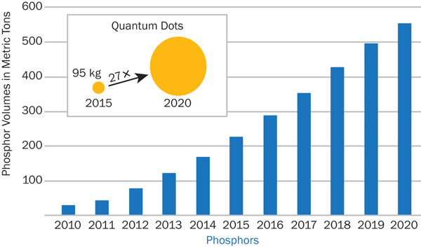
The growth of LED use in applications is being driven by and causing a growth in materials, such as a 27-fold increase in quantum dots for wavelength downconverters. Photo courtesy of Yole Développement.
The Lyon, France-based analyst firm forecasts an explosion in sales of LED materials, due in part to better performance in visually important aspects such as color rendering. Innovations in substrates and phosphors lie behind such advances. These also benefit displays, where LEDs today are used primarily in backlighting for LCDs.
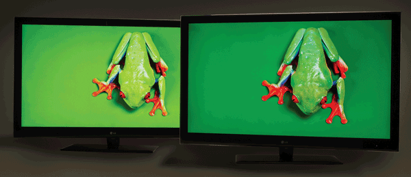
The use of quantum dots as an LED downconverter (right) enables deeper greens in displays in comparison with traditional phosphors (left). Photo courtesy of Nanosys.
Novel materials are powering the push of LEDs into new areas. For instance, according to Yole Développement, the market for ultraviolet LEDs will grow from $90 million in 2014 to more than $500 million and potentially much higher by 2019.
In many applications, LEDs face challenges involving heat and photon flux. One of the ways to deal with the first issue is to get more of the light out of the device and into use.
Light-emitting diodes are built out of compound semiconductors, with gallium nitride as the material of choice. Mixing in aluminum drops the emission wavelength, and the use of phosphors or other materials downconverts the emission into longer wavelengths.
Gallium nitride is grown on a substrate, with the most popular being sapphire. The industry is moving from substrates measuring 2 in. to those more than 6 in. across. Bill Weissman, CEO of leading sapphire supplier Rubicon Technology Inc., said that the Bensenville, Ill.-based company can produce substrates up to
10 in. across.

A 6-in. polished sapphire wafer (a), which is used as a substrate for LEDs. Patterning the sapphire substrates (b) with microstructures (c) improves light extraction and LED output. Photo courtesy of Rubicon Technologies.
The move to larger substrates is for economic reasons, he said. “It reduces the cost of the chip in two different ways. One is that larger substrates capture more of the chemicals in the MOCVD [metallorganic chemical vapor deposition] reactors and make that more efficient. And there’s less edge loss, meaning those little pie-shaped edges you lose from cutting square chips out of a round wafer.”
Another approach that reduces cost is to pattern the substrate. Patterning creates miniature structures that more efficiently guide the light out of the device and keep it from being absorbed. This can increase the amount of light extracted by as much as 30 percent, Weissman said. That makes the LED more efficient, and it also can reduce the cost by, for example, allowing the use of a less expensive heat sink. Other substrate choices such as silicon, aluminum or gallium nitride exist, but the majority of LEDs today use sapphire.
Materials innovations
An emerging substrate possibility is graphene. Technology using this material for the growth of light-emitting semiconductor nanowires is under development by CrayoNano AS, a Trondheim, Norway-based startup. The sheets of carbon atoms that make up graphene offer some advantages, said CrayoNano Chief Technology Officer Helge Weman.
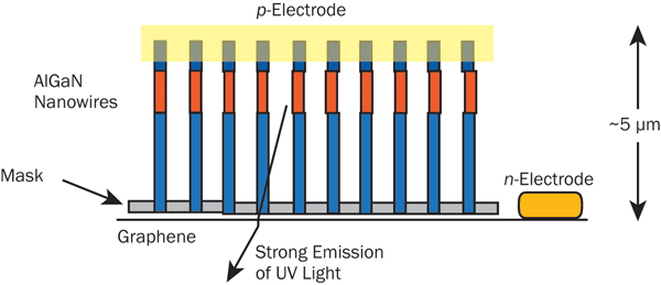
Schematic of semiconductor nanowires grown on a graphene substrate, which could result in deep-UV (265 nm) LEDs that are useful for sterilization. Photo courtesy of CrayoNano.
For one thing, there is very little lattice mismatch between graphene and the semiconductors, an important plus because mismatch causes performance-robbing defects to form. Also, graphene is a good heat conductor and can be used as a transparent electrode, which every LED must have.
But the real advantage of graphene becomes clear in the deep-UV, according to Weman. Graphene is transparent at such wavelengths, something not true of the materials commonly used in transparent electrodes and substrates. What’s more, good-quality aluminum gallium nitride, which produces deep-UV light, can be grown on graphene, something not easily done on other substrates.
Such advantages mean that graphene could be a breakthrough material enabling high-power LEDs in the deep-UV. As for applications, these include spectroscopy and medical uses. The biggest market, though, could arise from the location of a DNA absorption peak.
“We’re particularly aiming for 265 nm, which is perfect for sterilization and disinfection,” Weman said. The technology is in an early phase. Future plans involve first making a blue or near-UV LED on graphene, with a successful demonstration followed by increasing aluminum content until the emission sits near 265 nm. Delivery of the near-UV prototype could take a year or two, Weman said. Developing a successful deep-UV device will take a few years more.
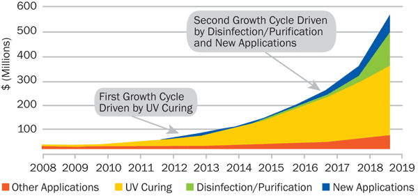
UV LED growth is expected to be strong, thanks in part to new materials that enable deep-UV and new applications such as disinfection and sterilization. Photo courtesy of Yole Développement.
Other LED innovations involve materials that downconvert light into longer wavelengths, transforming blue into green and red. Along with filters that
pass through specific wavelengths, this approach enables the full gamut of colors on a display. The balancing of red, green and blue also allows general illumination to range from warm to cool. With LEDs, it’s even possible to adjust this color temperature on command.
Green quantum dots, tunable from 530 to 550 nm center wavelength. Photo courtesy of Quantum Materials Corp.
Downconversion means lost light and decreased efficiency, but material changes are helping reduce both. For instance, the human eye can’t see light beyond about 700 nm, so anything past that point is wasted, at least for general illumination and displays. Yet, traditional red phosphors have a relatively broad emission with a full width at half maximum of about 80 nm.
In contrast, potassium fluorosilicate (PFS) doped with manganese has an emission width in the red of 10 to 20 nm, according to a patent filed by General Electric. GE has licensed the technology for use in backlights, where the new phosphor provides advantages.
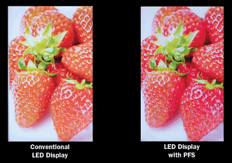
A new narrower-emission-width red phosphor (right) improves LED-backlit display performance over that of traditional phosphors (left). PFS = potassium fluorosilicate. Photo courtesy of GE.
“The addition of PFS into the package will increase the performance of the LEDs compared to LEDs that use other red phosphors,” said Gerald Duffy, general manager for global product management at GE Lighting. The East Cleveland, Ohio-based GE division makes lighting products for consumers and businesses.
In general-illumination applications, the new phosphors improve efficiency at a lower cost than would be the case with complicated LED drive electronics. However, GE has not licensed the technology for lighting.
It took years to develop the new phosphor, with much time spent making the material more robust under a wide range of use conditions, Duffy said. Only when that was complete was it practical for use in packaged LEDs.
Enhancing LED efficiency
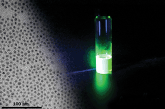
Quantum dots are another new downconversion material. Measuring a few nanometers across, quantum dots have a size-dependent emission with a half width of only nanometers. Along with efficiencies that run 97 percent, such attributes make them useful in LEDs.
Quantum dots being fabricated and tested. Photo courtesy of Nanoco Technologies.
Nanosys Inc. of Milpitas, Calif., makes quantum dots, putting them into polymer films that can be dropped into the standard LED manufacturing flow. The polymer acts as both a structural material and a protective barrier so that the quantum dots are not damaged by oxygen or moisture.
The company’s red- and green-emitting quantum dots improve LED efficiency, thanks to a full width half maximum under 30 nm. “That enables us to match the spectrum of the backlight to the color filters. That means we’re not spending any energy generating light that doesn’t go through,” said Jeff Yurek, product marketing manager.
While quantum dots are gaining ground as downconvertors for LEDs in displays, they face challenges in general illumination. One issue is heat, as it is necessary for the quantum dots to be closer to the LED than is the case in displays. They also could be subject to high heat during LED manufacturing, said David Doderer, vice president for R&D at San Marcos, Texas-based Quantum Materials Corp. The company has, therefore, been refining its quantum dots to satisfy these requirements.
“We’ve done internal testing for brief temperature spikes, as well as longer-term aging testing. Both of those are on really good tracks,” Doderer said. “If quantum dots perform well when placed close to the LED, then other aspects of the system can be optimized.”
One possibility would be a reduction in the overall size, leading to low-profile devices that are not just replacements for standard lighting. Such flexibility and the capability to tailor lighting output could allow adjustable lights to optimize growth for urban agriculture and other novel applications.
Getting quantum dots very close to the light-emitting area of an LED chip could enable smaller and thinner lighting products than are possible today, said Steve Reinhard, vice president of the Manchester, UK-based Nanoco Group plc. However, doing so might require a significant material change and a more complex, and possibly more expensive, particle. On the other hand, less of the material would be needed.
Today, Nanoco makes a product for general illumination that combines a green phosphor with a red quantum dot. The result is a warm light with a high CRI,
or color rendering index, Reinhard said.
Even as quantum dots improve, they may never totally replace more traditional phosphors in LEDs. In displays, narrowband emission is a performance and efficiency plus due to the presence of color filters. In lighting, broad emission, especially in the green, is an advantage because of how the eye works.
Phosphors already provide broad emission. It’s possible to duplicate this using three or possibly four different-sized quantum dots. However, quantum dots are broadband absorbers and narrowband emitters. Thus, the various quantum dots would get in each other’s way, in a photon absorption-emission sense. That reality places a requirement of near perfection on the many types of quantum dots in such an LED.
Discussing this material challenge, Reinhard said, “There’d be too many losses, unless you’re 100 percent efficient.”