MOSCOW, Russia, Jan. 19, 2016 — A femtosecond laser deposition mechanism has achieved patterns on glass with 100-nm resolution. The method could allow quick and inexpensive production of nanoscale sensors and chips.
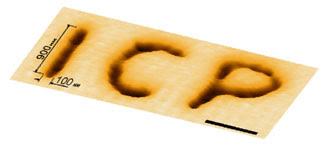
Institute of Chemical Physics abbreviation applied to glass. Courtesy of ACS Publications/Applied Materials & Interfaces.
The work resulted from a joint study by the Moscow Institute of Physics and Technology, Institute of Chemical Physics, Moscow State University, and the Institute of Problems of Chemical Physics.
Femtosecond lasers are often used to deposit complex 2D and 3D patterns on the surface of transparent materials but offer limited resolution and are therefore limited in their abilities to produce nanoscale patterns.
To improve resolution, the near-field effect is often used in conjunction with a laser, which involves focusing a laser beam using metal nanoparticles or a layer of dielectric microspheres as a lens. This method, the researchers said, complicates the pattern’s deposition process, as the lens is fixed in space.
The Russian team’s method involved using a beam of light in fluid to create a trap where they placed glass microspheres. The trap could be moved, thereby moving the lens in space and focusing the laser to the desired area of the glass.
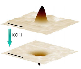
The laser-treated surface of the glass before and after the application of alkali.Courtesy of ACS Publications/Applied Materials & Interfaces.
Exposing the material surface to the laser enabled the creation of hillocks — but not craters — that were rough and wide. Adding alkali at a temperature of 90 °C turned the hillocks into smooth craters with resolution below 100 nm. One-step structuring, when the surface is treated only with a laser, does not allow resolution below 150 to 200 nm, depending on the complexity of the structure, the researchers said.
In addition to direct patterning process, the scientists investigated dependence of the resolution on the laser power. They reported that to obtain greater precision, it was more effective to use small spheres.
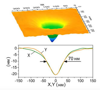
Image of the smallest crater (70 nm). Courtesy of ACS Publications/Applied Materials & Interfaces.
To demonstrate their method, the abbreviation of the Institute of Chemical Physics (ICP) was deposited on glass with a resolution of about 100 nm and an average depth of 20 nm. The minimum reported width of a crater created with the method was 70 nm.
The research was published in Applied Materials & Interfaces (doi: 10.1021/acsami.5b09454).