Editor’s Note: This is the inaugural edition of EPIC Insights, which delves into advances and issues facing the photonics market throughout the European Union. It’s authored by the European Photonics Industry Consortium (EPIC).
JOSE POZO, EUROPEAN PHOTONICS INDUSTRY CONSORTIUM (EPIC)
The next generation of biomedical and environmental sensors hinges on new discoveries in photonics technology. Yet years often pass from a promising discovery in the lab until commercialization, due to the lack of universally accepted design specifications, or limited access to the right manufacturing technologies — or any number of other factors.
This conundrum prompted the European Commission (EC) to act, forming a public-private partnership with Photonics 21 to create three open access pilot lines (see box for details) that will link supply chains from component design to integration in existing systems, and facilitate open access to industry through support services and tools, all of which will be validated through precommercial production.
The end goal: the rapid development of advanced sensors for environmental and chemical analysis; point-of-care diagnostics; tomography; superresolution microscopy; multiparameter vital sensors for wearables; and OLED-based displays and lighting systems for automobiles and buildings.
When is a mature technology … mature?
Top of mind for the initiative sponsors was identifying when a technology was truly mature enough for its industrial uptake. That may be trickier than it first appears as the nascent technology must withstand application-specific conditions — and for lengthy periods of time.
“In the last years, the emergence of mid-IR technologies for chemical detection has been supported by a number of EU-funded projects. The goal of [the pilot line] is the maturation of these technologies aiming at reducing the cost of fabrication by strong integration and miniaturization,” said Sergio Nicoletti, senior project manager at CEA-Leti in France and coordinator of MIRPHAB (mid-infrared photonics devices fabrication for chemical sensing and spectroscopic applications).
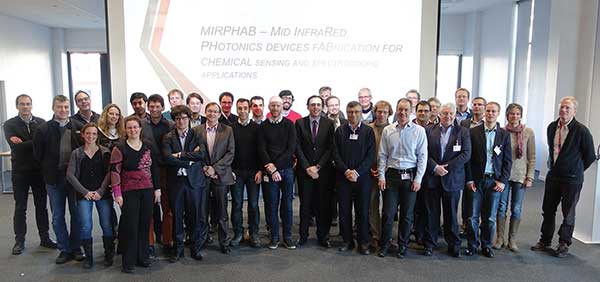
Kick-off meeting of the MIRPHAB project, hosted by coordinator CEA-Leti, in Grenoble, France, in January 2016.
MIRPHAB was launched in response to the growing need for more advanced sensing capabilities for environmental monitoring such as air and water quality. Other examples include sensors being developed for efficient breath analysis and the continuous analysis of body fluids, such as glucose monitoring.
In the past, the commercialization of mid-IR sensors has been limited to low-volume applications such as CO2 sensors in harsh environments. That will soon change with the evolution of civilization toward “smart cities,” creating a greater need for newer, advanced sensors and sensor networks capable of operating in the mid-IR range.
Creating new mid-IR sensors and lasers requires universally recognized fabrication libraries, specifications, design rules and definitions. Without rules, developers can’t design a product that can fit into the volume production process of the foundries. Standardizing procedure and creating process design kits, manuals and training will promote faster prototyping and fabrication activities. Moreover, the initiative will encourage input from European companies developing tools based on mid-IR sensors.
Integrated photonic circuits of tomorrow
For years the chief proponent of integrated photonic circuitry was the telecom industry. Because of this, circuits were designed to use wavelengths in the nonvisible portions of the spectrum. New and emerging biomedical applications, however, make use of the visible spectrum.
That has sparked interest in silicon nitride, which, in addition to being cost-effective and featuring very low propagation losses, is ideally suited for visible wavelengths. But silicon nitride devices must be connected to an optical fiber and assembled with electronics; there is no process or equipment available for this assembly today.
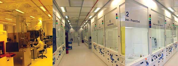
LioniX’s cleanroom facilities where silicon nitride-based photonic integrated circuits are manufactured.
Developing a single, generic platform from silicon nitride will also require the development of unique broadband building blocks or multiple similar building blocks for smaller wavelength bands.
While “the individual parts have been demonstrated to work for customers in the data/telecom domains, these are fairly different users,” said Arjen Bakker, CTO of Phoenix Software in the Netherlands, “so a key question is whether the same approach will work within this biosensing application domain.”
One successful past effort to lower costs and promote knowledge exchange is the Multi-Project Wafer (MPW) initiative. MPW will be an integral part of the PIX4LIFE access pilot, promoting the shared development of integrated photonic circuitry for health and food applications.

Chip designed and tested by VLC Photonics and fabricated using the MPW fabrication of LioniX. VLC Photonics and LioniX are partners in PIX4LIFE.
The MPW “is essentially a starting point for the R&D phase, prior to full production runs outside the scope of the pilot line running on mostly the same infrastructure, but handled mainly by companies rather than a mixed commercial/academic model,” said Bakker.
The pilot goes beyond wafer fabrication, however, aiming to bring together the full supply chain from design to the integration of the packaged chips in existing and future systems. This will provide companies with a single point of access for the entire process, from chip design to a packaged module. Customers can also create and share their own designs using the process development kits.
Measuring success
Here at EPIC we applaud the efforts of the European Commission and Photonics 21 in establishing the open access pilot lines. We pledge to use our global position to engage system integrators and end users alike to support the effort.
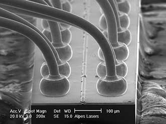
Scanning Electron Microscope (SEM) image of MIR laser using chip-on-carrier packaging technology with wire bonds. Manufactured by Alpes Laser, partner in MIRPHAB.
In the end, by enabling the proper maturity of the technology and the creation of self-sustainable pilot lines, we’ll all win, firmly establishing Europe as a leader in the global photonics market.
For the effort to succeed, participating firms must adopt an open
attitude, and must be willing to share specifications and knowledge they
would normally not share with a commercial, pure-play foundry. That
means participating in forums, sharing findings and informing one
another of market-driven specifications.
Acknowledgments
EPIC wishes to thank those who contributed their perspectives for this column; they include: Arne Leinse, vice president at LioniX (the Netherlands); Massoud Dadras, head of microscopy and nanoscopy at CSEM (Switzerland); Sergio Nicoletti, senior project manager at CEA-Leti (France) and coordinator of MIRPHAB; Antoine Müller, CEO of Alpes Lasers (Switzerland); Pieter Dumon, CTO of Luceda (Belgium); Twan Korthorst, CEO of Phoenix Software (the Netherlands); Joost van Kerkhof, CEO of XiO Photonics (the Netherlands); Arjen Bakker, CTO of Phoenix Software (the Netherlands); and Iñigo Artundo, CEO of VLC Photonics (Spain).
Meet the author
Jose Pozo is director of technology and innovation at EPIC (European Photonics Industry Consortium). He has 15 years’ background in photonics technology, market knowledge, and a large network within the industrial and academic photonics landscape. Pozo is a member of the board of the IEEE Photonics Society, Benelux. He holds a Ph.D. in electrical engineering from the University of Bristol, U.K., and a M.Sc. and B.Eng. in telecom engineering from Spain/Belgium.
Pilot Lines in Focus
• PI-SCALE — Applications include flexible OLEDs for lighting and signage
• PIX4LIFE — Photonic-integrated circuits for health and food applications
• MIRPHAB — Laser-based analytical mid-infrared (MIR) sensors for biomedical applications
Open Access for Small and Midsized Firms
One unique aspect of the initiative is the unprecedented access Europe’s small- and medium-sized enterprises (SMEs) will have to the manufacturing technologies developed, essentially leveling the playing field with their larger counterparts.
That competitive edge will spur commercialization of new innovative photonics-based products.
“Open access to the platform will be guaranteed to European SMEs and other research and industry partners. This way, many users will be able to design and prototype their optical systems using the advanced technologies proposed,” said Iñigo Artundo, CEO of VLC Photonics (Spain).
In order to maximize the impact and secure the sustainability of the pilot lines after completion, open access will be offered to out-of-consortium customers through a brokerage firm handling a list of products or solutions available for sale to the general public. These products will be components or integrated sets of components; they will also be specifiable as a black box or the customer may specify the integration of subcomponents to provide custom solutions.