
Laser Identifies Size, Shape of Materials for Quicker Optical Design
When optical diffraction was used to analyze the structure of a photonic crystal, researchers found that it created a characteristic light pattern that corresponded exactly to the number of scattering microscopic particles in the sample. The ability to determine the precise number of scatterings in optical materials has previously been done using electron or atomic-force microscopy only. A novel method for determining the properties of optical materials, done without the use of expensive microscopy tools, could help speed the design of optical devices.
A collaborative team of researchers from ITMO University, Ioffe Institute and Australian National University studied optical diffraction in 2D periodic photonic lattices. They observed strong optical diffraction from a finite number of elements and used this as a tool for determining the symmetry and exact number of particles in the sample.
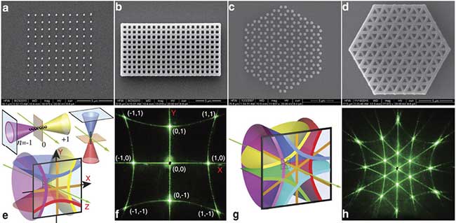
Examples of fabricated structures shown with scanning electron microscope (SEM) images: (a) direct square structure (10 × 10 voxels, a1 = a2 = 1 μm), (b) inverted rectangular structure with square symmetry (10 × 20 holes, a1 = a2 = 1 μm), (c) direct hexagonal structure (a = √3 μm ), (d) inverted hexagonal structure (a = 1.5 μm). (e) Schematic of the zero-order (n = 0) and first-order (n = ±1) Laue diffraction from the horizontally and vertically oriented chains of scatterers and from the structure with square symmetry composed of both types of chains in the case a1 = a2. Diffraction patterns on a flat screen are shown by thick lines. Scattered light is shown by different colors for clarity. (f) Experimental pattern for diffraction of monochromatic light (λ = 0.53 μm) from an inverted structure of the square symmetry (100 × 100 holes, a1 = a2 = 1 μm) observed on a flat screen positioned behind the sample. Main diffraction maxima are marked with the pairs of the diffraction indices (n1, n2). (g) Schematic of the zero- and first-order Laue diffraction from the hexagonal structure. (h) Experimental pattern for zero-, first- and second-order Laue diffraction of monochromatic light (λ = 0.53 μm) from an inverted hexagonal structure (a = 1.5 μm) observed on a flat screen positioned behind the sample.
“The light senses heterogeneity,” said Mikhail Rybin, researcher at the Department of Nanophotonics and Metamaterials at ITMO University. “Depending on the shape and relative position of the scatterers, the light wave continues to propagate differently behind the sample. In other words, the structure of the sample affects the diffraction pattern, which will be projected on the screen. We found out that by looking at the pattern it is possible to determine the precise number of scatterers in the material. This helps understand not only the type of the sample lattice (square, triangular), but also establish its structure (20 to 20 particles, or 30 to 15) just by counting the light spots on the screen.
“In addition, our method makes it possible to study optical materials without changing their structure, in contrast to electron microscopy, where the sample surface has to be covered with a conductive metal layer, which impairs the optical properties of the sample,” he added.
The researchers used a direct laser writing (DLW) technique to fabricate a variety of high-quality finite-size 2D photonic structures with submicron-scale features. They fabricated both direct and inverted dielectric photonic structures as 2D periodic arrays of scatterers with the square C4v, orthogonal C2v and hexagonal C6v lattice symmetries. The direct photonic structures were composed of dielectric particles with an ellipsoid-like shape with a typical size of 100-300 nm in the surface plane.
When they studied optical diffraction from fabricated direct and inverted finite-size 2D structures they observed a variety of diffraction patterns. They were able to detect scatterers in any direction.
They also investigated the transition between two main classes of optical materials: photonic crystals and metasurfaces; and they determined the lattice parameters that define whether the light perceives the material as a 2D photonic crystal or a metasurface. Using a set of anisotropic samples with orthogonal C2v lattice symmetry, the researchers demonstrated the transition from a multi-order diffraction system typical of photonic crystals to a system where only the zero-order diffraction could be observed.
They found that in both photonic crystals and metasurfaces, the scattering particles were arranged in a flat lattice. However, in the case of a 2D photonic crystal, the light perceived the sample as a set of separate particles and generated an intricate pattern on the screen behind the sample when light passed through the sample. In the case of a metasurface, the light perceived the sample as homogeneous, and the screen showed only one spot, indicating that the scattering particles were located too close to each other to be perceived as separate. The light passed through the metasurface sample without splitting.
In order for the light beam to pass through a metasurface, the distance between the particles must be smaller than the wavelength of light. However, metaproperties will often manifest when the distance between the particles is larger. It is useful to find the maximum allowable distance, since reducing the structure by a single nanometer can make the technology more expensive.
The research was published in Scientific Reports (doi:10.1038/srep30773).
Published: September 2016