A photodetector that is ten times smaller than current standard silicon diodes has been developed using molybdenum disulfide (MoS2) sandwiched between two graphene sheets. The 2D device, which has just one layer of MoS2, demonstrated the ability to produce more photocurrent than comparable multilayered devices, even though it absorbed less light.
To discover the reason for this surprising result, researchers from the Institute of Basic Science (IBS) compared photovoltaic devices with one layer of MoS2 with devices with seven layers of MoS2, and tested how well the devices were able to convert light into an electric current. Researchers found that although the device with one layer of MoS2 absorbed less light than the one with seven layers, it had higher photoresponsivity.
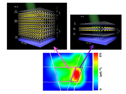
Devices with one-layer and seven-layer MoS2 were built on top of a silicon base and compared (top). The device with one-layer MoS2 (inside the violet box) showed better performance in converting light to electric current than the seven-layer device (inside the pink box)(bottom). Courtesy of IBS.
"Usually the photocurrent is proportional to the photoabsorbance; that is, if the device absorbs more light, it should generate more electricity, but in this case, even if the one-layer MoS2 device has smaller absorbance than the seven-layer MoS2, it produces seven times more photocurrent," said researcher Yu Woo Jong.
The results could not be explained through classical electromagnetism; but an explanation could be found in quantum physics. The thinner device could generate more current because it had more electrons flowing in the same direction.
When light hit the devices, some electrons from the MoS2 layer entered an excited state and flowed through them, producing an electric current. In order to pass through the boundary between MoS2 and graphene, the electrons needed to overcome an energy barrier. This was done through quantum tunneling.
Theoretical modeling showed that asymmetric potential barriers in the top and bottom interfaces of the graphene/one-layer MoS2/graphene heterojunction enabled asymmetric carrier tunneling, causing high photoresponsivity in the one-layer MoS2 device.
The bottom SiO2 layer of the devices increased the energy barrier, while the air on top reduced the barrier. This gave the electrons in the monolayer device a higher probability of being able to tunnel from the MoS2 layer to the top layer of graphene (GrT). In the monolayer device, the energy barrier at the GrT-MoS2 junction was lower than the barrier at the junction of the bottom graphene layer (GrB) and MoS2; so the excited electrons transferred preferentially to the GrT layer and created an electric current.
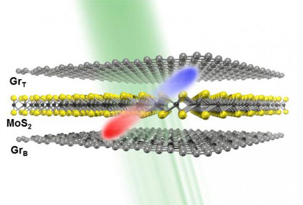
Illustration of the device with the molybdenum disulfide (MoS2) semiconductor layer sandwiched between top (GrT) and bottom (GrB) graphene layers. Light (green ray) is absorbed and converted into an electric current. When light is absorbed by the device, electrons (blue) jump into a higher energy state and holes (red) are generated in the MoS2 layer. The movement of holes and electrons created by the difference in electronic potential between the GrT-MoS2 and the GrB-MoS2 junctions generates the electric current. Courtesy of IBS.
In contrast, in the multilayer MoS2 device, the energy barriers between the GrT-MoS2 and the GrB-MoS2 junctions were symmetric. Therefore, the electrons in the multilayer device had the same probability of going to either side, which had the effect of reducing the probability of generating current.
Another reason why the thicker device could not generate more current is that electrons and the “holes” they create when they enter an excited state move slowly through the junctions between graphene and MoS2, leading them to recombine within the MoS2 layer in an undesirable way.
Spectral-dependent studies further showed that the internal quantum efficiency in one-layer MoS2 could reach a maximum of 65 percent, compared to 7 percent in seven-layer MoS2.
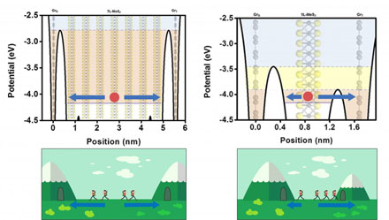
Mechanism to explain why the device with one-layer MoS2 generates more photocurrent than the seven-layer MoS2 one. In the one-layer device MoS2 (top right), the electron (red circle) has a higher probability to tunnel from the MoS2 layer to the GrT because the energy barrier (white arch) is smaller in that junction. In the seven-layers MoS2 device (top left) instead, the energy barrier between MoS2/GrT and MoS2/GrB is the same, so electrons do not have a preferred direction flow. More energy is generated in the one-layer MoS2 device because more electrons flow in the same direction (bottom). Imagine that people want to cross a mountain without too much effort. If the mountains have different height (right), more people choose to climb (or better, to tunnel) the small mountain, while if the mountains have the same height (left), they do not have a preferred route. (Graphics modified from Freepiks). Courtesy of IBS.
"This device is transparent, flexible and requires less power than the current 3D silicon semiconductors. If future research is successful, it will accelerate the development of 2D photoelectric devices," said Yu.
The novel device could be used in applications such as the Internet of Things, smart devices, wearables and optoelectronics.
The research was published in Nature Communications (doi:10.1038/ncomms13278).