Microelectromechanical systems hold promise for the development of commercial spectrometers for the broader market.
AHMED KORAYEM SAÏD, SI-WARE SYSTEMS
Chip-scale sensor integration has brought us to the edge of new market opportunities that are poised to transform business practices and consumer lifestyles. The ability to incorporate miniaturized sensors into small devices and broad networks means that actionable data can be collected anywhere, anytime — either on demand or on a continuous basis. This new capability enables consumers and businesses to monitor goods, conditions and operations in real time and to make changes and adjustments on the fly to optimize safety, health, quality control and production, and even care for the environment.
Nowhere is this opportunity better illustrated than in the spectroscopy sector, where miniaturized technology is poised to open vast new markets for a seemingly futuristic capability — instant and ubiquitous material analysis. Molecular analysis has long been associated with advanced science, laboratories and large equipment. However, we have now arrived at the age of the first chip-scale spectrometer for detection of material and analysis of chemical composition anywhere, anytime by nonscientists and consumers.
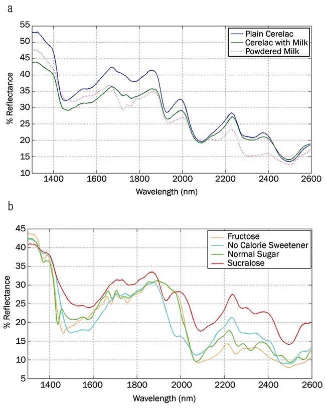
Measurements conducted on Cerelac infant cereal show the spectral signature for plain Cerelac and also the presence of plain milk and powdered milk in the mixture (a). Measurements of the ability to detect different kinds of sugars based on spectral signatures (b). Courtesy of Si-Ware Systems.
The development of spectroscopy-on-a-chip holds radical implications for many sectors because it dispenses with the time-consuming process of sending samples to a central lab for analysis. Instead, the “always on” capability means that individuals or businesses can detect the presence and percentage of targeted molecules at any time or continuously, whether detecting contaminants in a food production facility, quality control in pharmaceutical manufacturing, assessing alcohol in the bloodstream, or detecting volatile organic compounds (VOCs) in the home via the Internet of Things (IoT).
Near-IR spectroscopy
Near-infrared (NIR) spectroscopy has served to quantify and qualify materials for many applications. Using NIR, a device can derive a spectral signature from a particular material by shining a broadband light on a sample and measuring its spectral response. The spectral response provides a reference for performing identification and/or quantification analysis using predeveloped analysis models.
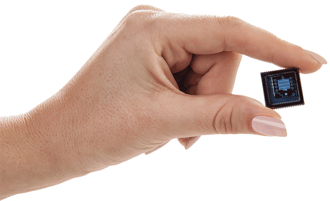
The NeoSpectra Micro spectral sensor for mobile device applications is scheduled for volume production this year. Courtesy of Si-Ware Systems.
NIR differentiates itself from other approaches by generating accurate data immediately on multiple chemical and physical parameters at the same time. No preparation of different sample types is required. While wet chemical and other conventional analysis methods can demand a delay until certain transformations occur in the sample, with NIR this need is eliminated. NIR light can even pass through plastic and glass to provide analysis of materials inside a package or container.
While NIR spectroscopy can provide significant advantages including quick results and some portability for on-site use, technical and market barriers have severely limited the development of versatile tools for expanded commercial use, not to mention consumer use. In the case of a consumer device, the obvious prerequisite is miniaturization that can enable integration into an easy-to-carry mobile device form factor.
Price point and scalability are also a challenge: Recent prices have hovered between $10,000 and $20,000. Much more integration is required to make manufacturing scalable to hundreds of thousands of units. Given the need for robust, high-accuracy optics and circuitry, there is no choice but to move toward semiconductor-style manufacturing. In essence, spectrometers must be as cheap as chips.
Engineering teams have tried a variety of techniques to achieve better integration and smaller form factors for a NIR device, including micromirror arrays, linear variable filters, tunable Fabry-Perot filters and other approaches. These advances have helped move spectrometers toward a module size for some portability, but even more versatility is required for nonexpert use, including an increase in spectral range for a single sensor. The question is: What approach can get the industry to a chip-scale size with the necessary capabilities?
MEMS: A key to the consumer market
MEMS (microelectromechanical systems) holds great promise for the development of an FT-NIR (Fourier transform near-infrared) device that meets the major requirements for the broader market. For devices with moving parts such as mirrors, MEMS has an established track record and offers a major advantage over other approaches: miniaturization to chip scale, use of semiconductor style wafers, and etching techniques for high-volume batch-style production, ultimately providing pricing at the component level.
The ability to develop moving structures at microscale that can be produced in high volumes and at wafer-scale cost has opened the door to new untapped markets, a recent example being the motion-sensing accelerometers found in smartphones, automobiles and other consumer equipment.
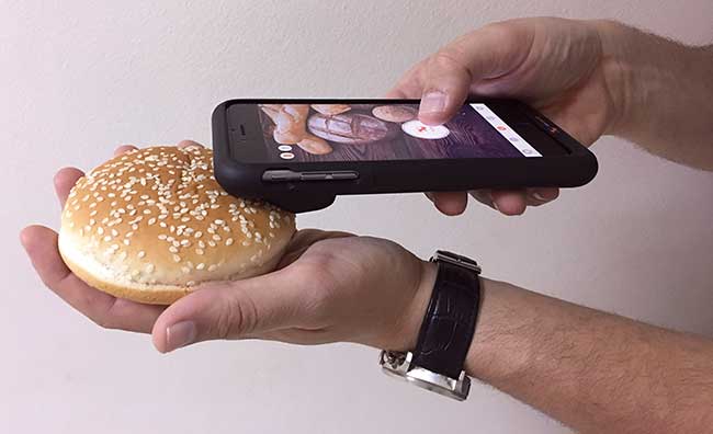
A prototype application for detecting gluten with a smartphone, using software developed by GreenTropism and a case developed by Xpndbls. Courtesy of Si-Ware Systems.
Si-Ware Systems has developed a variety of MEMS capabilities through its combined work in MEMS, ASIC development and photonics, and through the creation of a proprietary technology called SiMOST (Silicon integrated Micro Optical Systems Technology) that enables the replication of semiconductor capabilities for the photonics industry. The technology pulls from a library of well-characterized and validated optical and mechanical components to design and fabricate optical benches — on a single silicon chip. The team used this technology to develop a fully monolithic Michelson interferometer with moving mirrors.
The Michelson interferometer, the core of any FT-NIR spectrometer, is an optical interferometer. A beamsplitter splits the incident beam into two paths: One of the beams is reflected by a moving mirror and the other is used as a reference when reflected by a fixed mirror. The moving mirror controls the optical path, or simply the delay, of the first beam and thus the two reflected beams interfere, producing a pattern that corresponds to the spectral content of the input light. The latter is captured by the single photodetector, generating an “interferogram.” The spectrum of the input light is directly generated by applying a Fourier transform over the interferogram.
The three-dimensional SiMOST spectrometer design is printed onto masks in the same way that other MEMS devices are produced. These masks pattern the design onto silicon wafers by photolithography. The patterns are subsequently etched in layers, using batch processes. The chips are then diced and packaged, enabling unprecedented economies of scale that significantly lower costs.
The scanning electron microscope photo of the miniaturized version of the Michelson interferometer shows all the optical components (fixed mirror, moving mirror and beamsplitter) as well as the mechanical components (a MEMS comb drive micro-actuator) integrated onto the single chip. The components are aligned using a single photolithography process. They are fabricated with a single deep reactive ion-etching (DRIE) process.
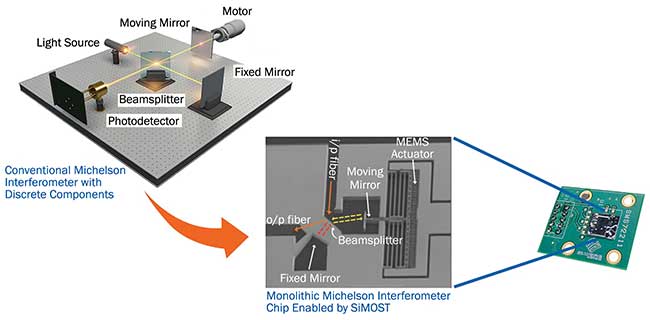
A conventional Michelson interferometer and a MEMS-based interferometer-on-a-chip. Courtesy of Si-Ware Systems.
The dedicated ASIC chip complements the functionality of the interferometer, resulting in the creation of a full spectrometer. It achieves this by generating the electrical signals that drive the MEMS micro-actuator. The ASIC also reads data from the photodetector and performs signal conditioning functions as well as using digital signal processing on the measured data (optical signal and mirror position) to generate the spectrum.
In conventional FT-NIR spectrometers, an HeNe laser system detects the moving mirror’s position: By detecting the laser beam reflected by the moving mirror, the mirror’s position can be accurately determined. The MEMS version uses a novel technique facilitated by the ASIC chip, where the capacitance of the comb drive is sensed. This capacitance variation is related to the moving mirror’s position.
Performance advantages
FT-NIR devices require only a single photodetector to capture the optical power, which differs greatly from spectrometer instruments based on grating/dispersive techniques that require detector arrays including large numbers of detection elements (128, 25, 512 or 1024, depending on the required resolution).
With conventional FT-NIR instruments, the operating wavelength range is constrained by the materials of the beamsplitter and the photodetector in use. The MEMS version calls for the beam to be split using a single medium interface (silicon/air). Such a technique offers a stable splitting ratio over a very wide spectral range. As a result, the operating wavelength range depends only on the photodetector in use. Covering wide ranges at the higher end of the NIR spectrum (higher than 1150 nm up to 2500 nm) means different materials can be measured simultaneously with high accuracy. In addition, it allows measuring samples in different form factors ranging from particles to flat surfaces and even ground samples, with no need for sample preparation. The wide range offers a fit for many industries.
The resolution at a given wavelength is a function of the maximum achievable optical path difference (OPD) between the two beams, meaning that an instrument’s resolution is mostly contingent on the maximum travel range of the moving mirror. For a given MEMS actuator, the stroke of mirror can be adjusted by applying the appropriate electrical signal. Hence, resolution of the spectrometer can be easily adjusted.
Ubiquitous spectral sensing
Using MEMS to achieve new size, integration and scalability requirements for material analysis opens up vast new user opportunities for many sectors of the marketplace, both on the production and the consumer side. The ability to integrate chip-scale spectroscopy devices enables the development of “always-on” mobile or small form factor spectroscopy devices for in-line manufacturing and quality control, as well as on-demand applications that can be used in the field.
On the production and quality control side, such applications promise to be tremendously important for chemically sensitive operations that now require shutdown and delays when contamination or inconsistencies are even suspected. Food processing, pharmaceutical manufacturing, oil and gas refineries — such industries all offer prime targets for spectroscopy adoption.
On-demand spectroscopy, which includes consumer applications, may provide an even larger opportunity. The ability to carry a cellphone-based analysis tool or attached device anywhere, anytime introduces the ability to assess food in stores, restaurants and homes for ripeness, spoilage or allergens. In the medical arena, consumers or clinic staff could detect the presence of certain compounds through skin or in blood. Consumers or pharmacists could check medications before or after purchase to verify ingredients and to ensure they have not been given someone else’s prescription.
To date, such applications have been unavailable due to the cost, size and scalability of spectral sensors. In this new era, MEMS-based FT-NIR spectral sensors surpass these challenges and open the door for new applications that have only been imagined.
Meet the author
Ahmed Korayem Saïd is product marketing lead for NeoSpectra for Si-Ware Systems. Saïd received his bachelors in electrical engineering from the French University in Egypt, and his M.Sc. in electric and computer systems from the University of Pierre & Marie Curie (UPMC). He has served as technical marketing lead for the MEMS FT-IR spectral sensor NeoSpectra module and the chip-scale NeoSpectra Micro from R&D through volume production; email: [email protected].
From Quality Control to Health Monitoring
To capitalize on the potential of this technology to allow for a small, low-cost and scalable NIR spectral sensor, a chip-sized spectral sensor module was developed. The photodetector, the MEMS chip and the ASIC chips have been housed under one roof in a single 18 × 18-mm package. The smaller footprint enables the creation of new usage models and applications for spectroscopy. Portable spectrometry, in-line process monitoring, wireless spectrometry networks under an IoT umbrella, and integration into mobile consumer devices are just a few examples. Each of these usage models can include qualitative and/or quantitative analysis of materials in different sectors including medical, industrial, food and beverage, forensics, and law enforcement applications.
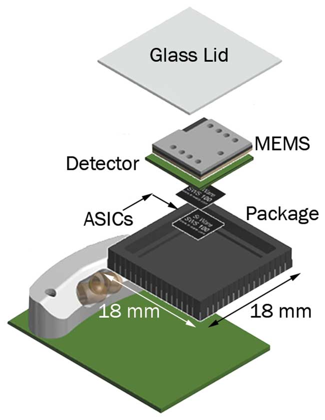
Exploded view of the spectral sensor in a chip-scale package. Courtesy of Si-Ware Systems.
Portable soil analysis
As an example of a new usage model made possible by the smaller FT-NIR form factor, a company called SoilCares, in the Netherlands, has incorporated the FT-NIR-based spectrometer into a ruggedized portable instrument for field use. The tool includes a wide steel tube to plunge into the soil to secure a representative sample. When the button is pushed, the scanner activates, obtains the soil signatures and relays them via mobile phone to a cloud-based database for a determination on the amount of nitrogen, phosphorus, potassium and many other ingredients contained in the soil. The SoilCares scanner now eliminates the tedious procedure of collection and delivery of soil samples by enabling in-field soil analysis.
Oil & gas quality control
An oil refinery needed to set up cost-effective spot-checking on a refinery production line. Rather than having to send samples to an onsite or offsite lab, the company used a compact FT-NIR engine to create a portable instrument that can scan oil and gas samples at various stages of production to ensure the right blend and consistency.
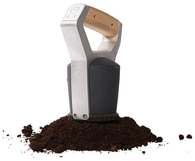
The SoilCares portable soil spectrometer, built around the MEMS-based Fourier transform-NIR spectral sensor, measures soil quality based on nitrogen, phosphorus and potassium levels, as well as other soil conditions. Courtesy of SoilCares.
Medical
A medical firm in Utah decided that there had to be a more convenient and more accurate way for prediabetic patients to ascertain glucose levels and potentially delay onset and progress of the disease. They saw significant potential using near FT-NIR spectroscopy to conduct instant urinalysis within a toilet — meaning no disruption to patient routine. A light source illuminated the sample in the slot and the FT-NIR device measured the glucose. The device was able to display either a target range of glucose or an optimized indication of sharp upward or downward trends.