Exploiting the unusual optical properties of very small objects, quantum-based technologies are starting to revolutionize lasers, solar cells, communications and more.
Smaller is often better, as it frequently can reduce the size and weight of gear while cutting power consumption and boosting performance. However, going small requires photonics innovations in the form of new materials, manufacturing techniques, configurations and other factors. Examples can be seen in innovations based upon quantum effects, the sometimes spooky rules that govern the very smallest objects.
A case in point comes from QD Laser Inc., a Kawasaki, Japan-based company that makes quantum dot lasers. In these devices, the optical gain material is made of quantum dots – semiconductor nanocrystals measuring a few tens of nanometers. These ultraminiature particles exhibit a unique behavior.
“Due to three-dimensional electron confinement in the quantum dot structure, electron energy states become discrete, similar to those of individual atoms,” said Dr. Mitsuru Sugawara, president and CEO of QD Laser.
This atomlike behavior leads to discrete energy levels, and this means that thermal broadening is restricted, according to Sugawara. Hence, lasers constructed using this technology work in a way that is fundamentally independent of temperature from −40 to 100 °C, which is not possible with other optical gain materials.
The technology has been used to mass produce lasers for data communications, with QD Laser shipping more than 1.6 million chips. The technology also has been applied to silicon photonics. In chip-scale silicon photonics, the temperature may vary according to how hard a particular part of the overall chip is working, which makes insensitivity of the optical link to temperature swings beneficial.
Other applications are downhole for underground exploration of natural resources. The lasers’ ability to operate at temperatures up to 200 °C is a key advantage here.
“This realizes low-power, temperature-stabilized and also high-temperature operable laser diodes,” Sugawara said.
QD Laser produces quantum dots by directing beams of indium and arsenic atoms onto a gallium arsenide substrate. The deposited atoms form crystals. Due to the strain created by a lattice mismatch with the substrate, the crystals aggregate to form quantum dots that measure about 20 nm across and 5 nm high. The quantum dots emit and absorb light at about 1300 nm, a wavelength useful in communications.
The size of the quantum dots and the strain they experience set the wavelength of the resulting laser. The optical gain is a function of the density of the quantum dots, with this made greater through the use of multiple layers of the material. QD Laser is working to increase dot density and thereby up laser performance, according to Sugawara.
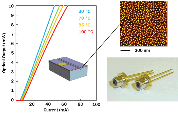
Lasers that use quantum dots (upper right) as an optical gain material are insensitive to temperature (left), potentially allowing them to drop temperature control components and to miniaturize. Photo courtesy of QD Laser.
Temperature insensitivity can help lasers miniaturize, he added. Currently, standard lasers incorporate technology to counter temperature changes, and this adds to the size of such lasers and to the power they require. Stable optical performance across a wider temperature range means temperature control is not needed.
As for the future, the technology could be applied to – and possibly help miniaturize – other devices. “The quantum dots at QD Laser are fabricated through self-assembling technology on semiconductor substrates and can be sandwiched by conductive semiconductor layers. So they can be applied to optical detectors at certain wavelengths,” Sugawara said.
Quantum dots are also being applied to other emission and absorption devices. An example comes from QD Vision Inc. This Lexington, Mass.-based company makes quantum dots that consist of a cadmium selenide core enclosed within a zinc-cadmium selenide shell, which renders the entire construct nontoxic despite the presence of the heavy-metal cadmium. The dots’ cores measure about 3.5, 4.5 or 5.5 nm, with the different sizes emitting in the blue, green and red, respectively.
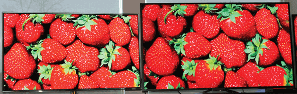
Two TVs, showing color quality with and without quantum dot technology. Photo courtesy of QD Vision.
QD Vision uses these quantum dots in displays and general illumination. In these applications, the new material replaces conventional phosphors, taking over the role of absorbing incoming blue light and then emitting the red and green needed to create a full range of colors. The new particles’ volume is a billionth of the old, with the switch to a more miniaturized material warranted because of superior optical performance.
“What’s really special about quantum dots is how bright, efficient and stable they can be. Their spectrum is extremely pure,” said Seth Coe-Sullivan, chief technology officer of QD Vision.
Indeed, the full width half maximum, or the width of the spectral output at half peak intensity, for these quantum dots is 30 nm, much smaller than the 60- to 90-nm equivalent of a phosphor. The narrower output is a benefit when used with a color filter, as it eliminates or minimizes leakage from one color channel to another. The result is that colors appear saturated.
QD Vision has a process that reduces the amount of quantum dots used, cutting it by 90 to 99 percent as compared to other implementations. In these alternative configurations, the quantum dots are applied as a film that covers the entire device surface. In QD Vision’s approach, the quantum dots are in what can be thought of as a straw sitting at the side of the device. This approach is possible because the company’s material can withstand higher temperatures and photon fluxes.
Looking forward, there is an opportunity to shrink quantum dot display and illumination components by perhaps a factor of 100, according to Coe-Sullivan. Today, quantum dots function as a phosphor substitute in a structure that is distinct from the light source. In the future, they could be incorporated to create a nanocomposite luminescent material. One way to do this was demonstrated in a 2012 Advanced Materials paper, which Coe-Sullivan co-authored.
The researchers etched and thereby textured the surface of a gallium nitride layer, creating holes into which they placed quantum dots. Doing so boosted the optical conversion efficiency to 82 percent, about that possible using the quantum dots alone. It also reduced the size of the overall structure by one or two orders of magnitude, to just that of what would be an LED chip itself.
One advantage of this integration is that it creates a more pointlike source. This is important for directional lighting and displays. However, getting from proof of concept to commercial production requires that the quantum dots be able to withstand much greater photon flux and possibly higher temperatures, both a consequence of being much closer to the pump light.
The industry is working on such improvements, according to Coe-Sullivan. “As the reliability and performance [go] up, you’ll be able to further miniaturize the quantum dot implementation in displays and lighting,” he said.
These and other expected advances are some of the reasons why analyst firm Touch Display Research forecasts that the quantum dot display and lighting market will reach $9.6 billion by 2023. That’s up from just $75 million in 2013.
Yet another quantum dot implementation comes from Quantum Materials Corp. of San Marcos, Texas. The company is a nanomaterials supplier, making tetrapod quantum dots. As the name implies, these quantum dots consist of a core and four arms. Adjusting the dimensions of either the core or the arms alters the spectral output, leading to the possibility of emission over a range of wavelengths and amplitudes.
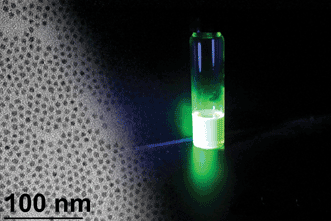
Green-emitting tetrapod quantum dots (left), when excited by UV light, produce bright-green light. The quantum dot display and lighting industry is forecast to be nearly $10 billion by 2023. Photo courtesy of Quantum Materials Corp.
Quantum Materials has produced quantum dots made out of heavy metals, such as cadmium, and is developing others with zinc and indium cores. An advantage of the latter is that the materials are nontoxic, which keeps potential toxicity issues from arising during manufacturing, use and eventual recycling.
Although the cost of quantum dots is confidential, there is some information that illustrates just how expensive these nanocrystals can be. The publicly known cost runs some $2000 a gram, 50 times as expensive as gold, according to Art Lamstein, director of marketing at Quantum Materials.
Such prices impact the use of quantum dots. However, Quantum Materials believes it has a solution to this problem. “We’ve developed and commercialized an automated process for the synthesis of quantum dots,” Lamstein said.
Besides substantially cutting the cost of production, automation brings another benefit, he added. It tightens the performance-defining attributes of the quantum dots by eliminating variations in size and shape introduced during manual processing. The result is that optical and other characteristics should be much more predictable, which could contribute to the yield of any product.
Quantum Materials has a subsidiary, Solterra Renewable Technologies, that is commercializing the technology in solar cells. These will be thin film and made in a roll-to-roll press, with the quantum dots embedded in a polymer using a proprietary process.
As for miniaturization, one possibility would be quantum dots sitting atop a conductive layer, Lamstein noted. Instead of working via photoluminescence, as all current quantum dot sources do, these devices would excite emission through electroluminescence. A key advantage would possibly be higher efficiency, as there would not be a multistep “electron to photon to downshifted photon” process by which the light is produced.
Such a device is an industry goal, according to Lamstein. Pulling it off would require creating a conductive and quantum dot layer such that electrons could be efficiently injected from the first to the second while keeping each intact. The quantum dot itself would need to be carefully crafted so that it would have a long life without developing surface defects and without the matrix developing heat-related color change.
“An electroluminescent device would be brighter, smaller, more efficient with less heat generated, less expensive to manufacture and open to many form factors. We think we have the material for it,” Lamstein said.
A final example of miniaturization and quantum effects comes from the emerging field of quantum communications and computing. Thanks to an ability to conquer what currently is effectively an unsolvable computation problem, such technology can crack most – and possibly nearly all – existing cryptographic codes. At the same time, this technology can also provide eavesdrop-proof communications.
A recent photonics breakthrough promises to shrink a key component. In October, researchers announced the generation of cross-polarized photon pairs on a chip-sized device. They did this by using two laser beams operating at different wavelengths and polarizations, sending these through a microring oscillator built out of a proprietary material. This generated photon pairs that could form the basis for quantum communications and computing. That will happen when photons are entangled, which will link them together via quantum mechanics in such a way that action on one will alter the other.
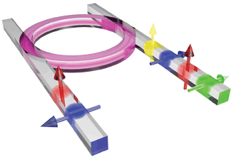
Using a microring, researchers for the first time produced cross-polarized photons on a chip-sized device, an important step in miniaturizing quantum computing technology. Photo courtesy of Lucia Caspani, Heriot-Watt University.
For such quantum effects to work, classical effects must be suppressed. The new research is the first time this has been done in a chip-sized device that is constructed with materials and in a manner compatible with modern semiconductor fabrication.
“You need a high-Q factor that allows you to have nonlinear effects at low pump power. This depends upon the material you choose and also your fabrication capabilities,” said Dr. Lucia Caspani, a fellow at Heriot-Watt University in Edinburgh.
Caspani co-authored a 2014 Frontiers in Optics paper on the research. At the time, she was working on the team of professor Dr. Roberto Morandotti at INRS-EMT in Canada. The next step in the ongoing research will be the transformation of the chip-sized device into an entangled photon source.
Eventually, the goal of researchers worldwide is to develop a chip capable of quantum communications and computation. For that, there are three elements that have yet to be demonstrated, said Dr. Chandra Natarajan, a postdoctoral researcher at the University of Glasgow, who is familiar with the field.
The first is the integration of source and detector – which could be a challenge, because most silicon-based sources run at room temperature, while promising detectors are superconducting and have to be cooled cryogenically. The second yet-to-be-demonstrated component is a fast reconfigurable element, which would enable the rapid alternation of photonic circuits based upon intermediate results. The third is some sort of memory, needed to store intermediate computation results. Finally, all of these must be on an integrated device and, hopefully, on the same chip.
That may sound daunting, but bits and pieces have already been demonstrated, which means that a miniaturized version of such devices may not be that far off. “In three to four years, a proof-of-principle chip is certainly possible,” Natarajan said.
ID Quantique is a Geneva-based supplier of quantum key distribution solutions that today are being used commercially. Patrick Trinkler, vice president of engineering, noted that the integration of quantum computing components onto a chip is important.
“Size and cost are the major roadblocks for a broad acceptance of quantum communication technologies. Developing dedicated photonics chips is certainly the best way to overcome these present difficulties,” he said.