Resolution, dynamic accuracy and throughput requirements will continue to drive nanopositioner makers in the coming year.
Scott Jordan, PI (Physik Instrumente) LP
Not long ago, nanometer-scale positioning was a laboratory curiosity. Today, the robust and responsive nanopositioning provided by piezoelectric actuation is more vital than ever in the lab and has become an essential commodity for industries ranging from semiconductor and disk-drive manufacturing to defense and the life sciences.
The semiconductor industry, for example, is animated by Moore’s law, which predicts a doubling of logic elements per unit area of silicon every 18 months. The disk-drive market’s bits-per-square-millimeter areal density curve has been even steeper in recent years. Likewise, microscopy applications have been increasingly dominated by requirements for optics with a high numerical aperture, and the formerly exotic technique of optical tweezers is spawning its first wave of industrial ventures.
The confluence of nanotech and industrial applications means that nanopositioning is colliding with economic prerogatives: Nanometer precision must be achieved in milliseconds because time is money to demanding nanopositioning users, who need higher resolution, faster settling, more on-the-fly processing, tighter synchronization with external processes, extraordinary fidelity to real-time position waveform patterns, more responsive communications, lower positional noise and better trajectory control.
Classical mechanics dictates an exponentiation of settling time as requirements become tighter — clearly an issue for cost-sensitive industrial processes as tolerances diminish. Moreover, besides the need for speed, economic prerogatives have pressured manufacturers of nanopositioning devices to accommodate larger-area processing. This necessitates longer-travel piezo-driven devices.
These requirements pose many conflicting goals. For example, consider a production engineer whose technical and cost goals urgently require automated, atomic force microscopy-class profiling of an ~1 mm2 device on the factory floor in one pass rather than a lower-resolution optical scan followed by a separate profiling of a small area, as is typically done. Furthermore, the profiling must be performed at a fast pace, with the scan plane flat to within <1 nm over the entire field.
These challenges are so extensive that perhaps even the term nanopositioning will no longer quite convey the collision of technical demands that will occur in 2007. The term nanoautomation more accurately captures the new, dynamic challenges facing the industry.
Emerging solutions
As voltage is applied to a piezo-ceramic actuator, a fairly linear expansion results (Figure 1). Hysteresis, nonlinearity and drift are addressed by closed-loop control that is based on a position-feedback device, such as a capacitive sensor or, for entry-level devices, a piezoresistive strain sensor.
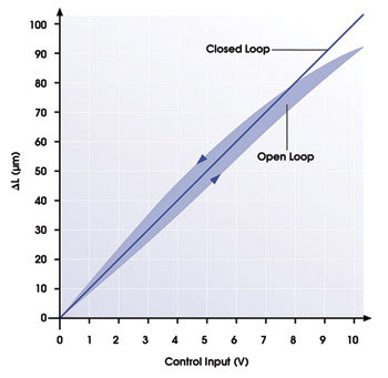
Figure 1. Open-loop actuation of piezoelectric nanopositioners is almost proportional to voltage. Closed-loop actuation linearizes the device.
The rough proportionality in Figure 1 means that the smallest motion that a given system can provide — its resolution — is proportional to the smallest voltage increment that the nanopositioning controller can generate. Because the commanding voltage is almost universally driven by a digital-to-analog converter, the smallest positioning step is limited by the converter’s granularity.
Unfortunately, longer-travel nanopositioning devices require increasingly larger motions because of the bit transitions generated by the digital-to-analog converter. For example, the popular converter cards from National Instruments Corp. of Austin, Texas, top out at 16 bits, meaning that they provide 216 (65,536) voltage steps. Therefore, a nanopositioner with several hundred microns of travel would provide only several nanometers of resolution when driven by such a card (Figure 2).
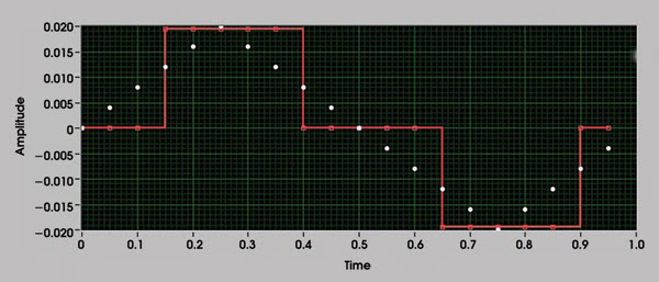
Figure 2. The bitness of a digital-to-analog converter limits how finely position can be controlled. White dots show the desired positions, while red lines show position approximations resulting from digital-to-analog converter granularity.
Higher-bitness converters are available but tend to be optimized for consumer applications rather than for instrumentation needs, with stability a common issue. Implemented in a digital controller inside the closed loop, stability is ensured, and with sophisticated waveform generation and fast interfaces as standard features of the best digital controllers, this is the best solution for resolving the travel-vs.-resolution issue. However, for many reasons, most customers still prefer to generate their position waveform externally. For example, the waveform generation and analog/digital and input/output synchronization capabilities of National Instruments’ LabView programming environment are very powerful.
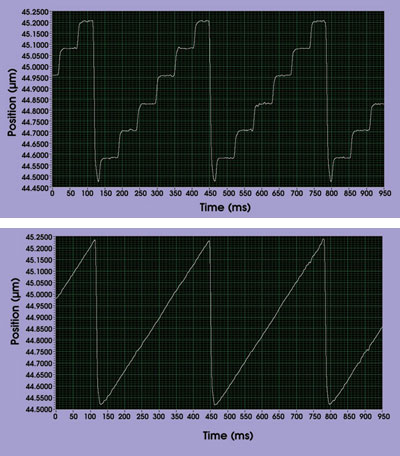
Figure 3. As measured by a laser interferometer, the position granularity resulting from the bitness of a digital-to-analog converter can be seen (top). A commercially available technology enables higher point-to-point resolution, better dynamic accuracy and a cleaner spectrum from real-time position waveforms (bottom), with no loss of positioning bandwidth.
Physik Instrumente’s HyperBit technology permits many additional bits of positioning resolution to be generated by almost any digital-to-analog converter, with no loss of bandwidth. Compatible with popular software and hardware architectures, and integrated into a LabView driver library for analog-interfaced applications, it can provide up to 11 bits of resolution on top of the converter’s native resolution, depending on the selected converter and motion device. These features virtually eliminate the converter’s contribution to the resolution-vs.-travel compromise.
Other problems
A servo may be defined as a mechanism that reacts to error to minimize it. This means that a certain amount of error is always present (or else the servo would do nothing). Between this fundamental property of positioning servocontrollers and the finite bandwidth and phase lags inherent in any electromechanical system, following errors — real-time departures from the desired position in on-the-fly motion patterns — can be significant. Traditionally, this places a speed limit on on-the-fly applications. The situation is complicated by the nonlinear behavior of piezoactuators, which require more sophisticated control techniques than do motorized devices. In particular, conventional feed-forward designs are inappropriate for piezos.
Following errors in repetitive motions such as those used in scanning and micropatterning can be essentially eliminated — reduced to approximately the noise level — using an algorithm called Dynamic Digital Linearization that optimizes the internal command generated for a repetitive waveform.
Advantages of piezo-based nanopositioners are their exceptional responsiveness and speed. A downside is that high dynamics can excite resonances in their load, supporting structure and adjacent components, causing a motion-driven “ringing.” Traditionally, this has necessitated dwells and “rounded corners” in the motion profile — both throughput killers. More recently, Convolve Inc. of Armonk, N.Y., developed Input Shaping, a technology that nullifies structural resonances by up to 95 percent, providing optimum throughput and improved dynamic accuracy.
In 2007, industrial nanopositioning applications will involve a continually advancing and sometimes contradictory mix of resolution, accuracy and throughput requirements. A deep tool kit of advanced technologies has been developed to provide researchers, integrators and engineers with the assurance that the performance they need will be available whenever they need it.
Meet the author
Scott Jordan is director of nanopositioning and nanoautomation technologies at PI (Physik Instrumente) LP in Auburn, Mass.; e-mail: [email protected].