Monolithic waveguide photodetector brings germanium’s photosensitivity to silicon photonics.
Cary Gunn and Gianlorenzo Masini, Luxtera Inc.
The introduction of very large scale integration dramatically cut the cost of electronic devices, driving the development of a wide range of new products. Efforts to bring the benefits of large-scale integration to the photonics sector have proved less than successful in the past. Now, with the development of monolithically integrated silicon-germanium photodetectors, photonic large-scale integration is poised to become a reality.
Waveguides, modulators, filters and couplers all have been integrated into silicon wafers but, until recently, little progress had been made with the integration of photodetectors. The stumbling block has been silicon’s relatively large bandgap, which renders it transparent — and hence a poor photodetector — at the infrared wavelengths of optical communication. Germanium, on the other hand, works well at these wavelengths and is compatible with silicon. The apparent answer has been to bring together these two materials but, until recently, this has been far easier to say than to do.
|
Glossary of Terms
CMOS
Complementary metal oxide semiconductor (CMOS) is a major class of integrated circuits. CMOS technology is used in chips such as microprocessors, microcontrollers, static RAM and other digital logic circuits. The technology also is used for a wide variety of analog circuits such as image sensors, data converters and highly integrated transceivers for many types of communication.
Flip chip
A flip chip — used for semiconductor devices such as integrated circuit chips — is one type of mounting that does not require any wire bonds. Instead, the final wafer-processing step deposits solder bumps on the chip pads that are used to connect directly to the associated external circuitry. This mounting also is known as the Controlled Collapse Chip Connection, or C4.
Monolithic integration
Monolithic integration refers to the integration of multiple devices into a single chip die. In this article, the term refers to integration of electronics and optics into a single CMOS die/chip.
SOI
Silicon on insulator (SOI) technology refers to the use of a layered silicon-insulator-silicon substrate in place of conventional silicon substrates in semiconductor manufacturing, especially microelectronics. SOI-based devices differ from conventional silicon-built devices in that the silicon junction is above an electrical insulator, typically silicon dioxide or, less commonly, sapphire. The choice of insulator largely depends on the intended application, with sapphire being used for radiation-sensitive applications and silicon oxide preferred for improved performance and diminished short channel effects in microelectronic devices. The precise thicknesses of the insulating layer and topmost silicon layer also vary widely with application. The first implementation of SOI was announced by IBM in August 1998.
Hybrid integration
“Hybrid integrated circuit,” “hybrid circuit” or simply “hybrid” is a miniaturized electronic circuit constructed of individual devices, such as semiconductor devices (e.g., transistors and diodes) and passive components (e.g., resistors, inductors and capacitors), bonded to a substrate or printed circuit board (PCB). Hybrid circuits often are encapsulated in epoxy. A hybrid circuit provides the same functionality as a monolithic integrated circuit, which in an end product serves as a component on a PCB. The difference between the two types of devices lies in how they are constructed and manufactured. In this article, “hybrid” refers to the integration of both electronics and optics into a single device.
Waveguide photodetectors
A waveguide photodetector (transducer that converts light signals to electronic signals) is integrated on the chip, as opposed to a discrete photodetector in a ROSA (Receiver Optical Sub-Assembly). In Luxtera’s case, a fiber connects to the chip via grating couplers. The light goes into the chip and then through a waveguide to a photodetector that is integrated into the chip. The photodetector then converts the light to electronic signals.
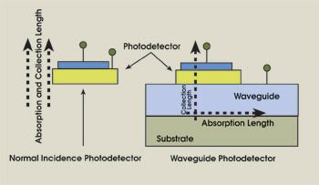 In the design of a surface-illuminated photodetector, a strong trade-off exists between collection (i.e., the distance that free carriers can travel before recombination) and absorption lengths: The former must be larger than the latter for good efficiency to be attained. Conversely, waveguide photodetectors relax this constraint by having light traveling perpendicularly to the direction of photon-generated carrier drift. This difference is exemplified in the figure at left. In the surface-illuminated (normal incidence) photodetector on the left, increasing the thickness of the absorption region increases both the collection and absorption lengths. In the waveguide photodetector on the right, the absorption length can be increased without affecting the collection length. In the design of a surface-illuminated photodetector, a strong trade-off exists between collection (i.e., the distance that free carriers can travel before recombination) and absorption lengths: The former must be larger than the latter for good efficiency to be attained. Conversely, waveguide photodetectors relax this constraint by having light traveling perpendicularly to the direction of photon-generated carrier drift. This difference is exemplified in the figure at left. In the surface-illuminated (normal incidence) photodetector on the left, increasing the thickness of the absorption region increases both the collection and absorption lengths. In the waveguide photodetector on the right, the absorption length can be increased without affecting the collection length.
| |
Now Luxtera Inc. has developed a process in which small deposits of pure germanium are added to the silicon wafer at the points where the light-to-electron conversion is required. The key benefit of this new process is that the germanium is added during wafer fabrication, providing significant gains in cost and efficiency.
Advantages of germanium waveguide photodetectors over other available types include integration, low cost, high yield, high reliability and small size. Germanium waveguide photodetectors enable the design of high-speed optical receivers with substantially better performance than that of any other available photo-detector.
The new process enables thousands of germanium photodetectors to be placed on a single chip, reducing the cost of each device from around a dollar to less than a penny. With this dramatic reduction, network and systems designers no longer will have to use photodetectors sparingly. This freedom will enable the creation and deployment of many new and unanticipated applications.
Moving forward
Today’s optical communication receivers use high-performance, discrete III-V (InGaAs) photodiodes, but these devices pose several drawbacks. Testing is possible only after the full receiver has been assembled and packaged, so defective wafers are not discovered until a very late stage of production. It would be better if testing could be performed on the wafers themselves so that defective ones could be discarded before further processing.
These devices are difficult to scale to multiple-channel applications because each channel requires a separate, expensive and large component. Moreover, performance is degraded because receiver sensitivity is limited by the capacitance of the bulky detector. Hybrid integration of photodetectors goes partway toward alleviating these problems because, in multichannel applications, flip-chip devices are smaller than packaged devices and can be mounted in proximity on the same chip.
However, monolithic integration allows for wafer-scale testing and improves performance thanks to the much smaller capacitance of the individual waveguide detectors. And, from an economic perspective, costs per die barely increase as the number of detectors on the die grows into the hundreds or even thousands. This enables easy channel-count scaling, better controllability and innovative architectures.
There are a number of key challenges to integrating germanium photodetectors onto the CMOS wafer successfully. Size is important: For one thing, the photodetector must fit physically into the space allowed for a CMOS transistor, which is much less than a micron thick. A surface-illuminated device cannot be used because such devices are typically a few microns thick. A waveguide detector, on the other hand, can be as thin as a modern CMOS transistor.
The thermal budget available for the growth of germanium is limited because a process that is too hot will damage other existing devices on the silicon wafers (transistors and interconnects). We have developed a low-temperature process that fits into a standard CMOS wafer fabrication flow and that does not affect performance of transistors or other optical devices.
Another key problem is that germanium has a 4 percent lattice mismatch with silicon, making material growth quite challenging. The direct growth of germanium on silicon results, in fact, in the formation of small islands where the germanium atoms preferentially pile up.
This clearly is unacceptable from a device standpoint and can be avoided by using an appropriate buffer layer between the silicon and the germanium. The buffer layer must be thick enough to serve its structural purpose and must be applied at a sufficiently low temperature to avoid damage to other components on the chip.
Saving money
There are significant financial benefits to be derived from embedding the photodetectors rather than surface-mounting them. Surface-mounting would require expensive pick-and-place processes whose costs would scale with the number of devices. Conventional optics manufacturing costs primarily are driven by assembly yields and by the cost of materials and of testing.
An integrated photodetector significantly reduces the costs for all three areas. Embedding the photodetectors directly into the wafer eliminates the costs associated with assembling and testing multiple components. This technology will allow a practically unlimited number of photodetectors to be grown directly on a die during wafer manufacturing at one common manufacturing step, reducing the overall materials cost. Also, the complete optoelectronic receiver solution can be tested economically at the wafer scale. Figure 1 shows a magnified photo of an integrated photodetector that is less than 40 square microns.
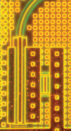
Figure 1. This self-contained photodetector occupies an area less than 40 square microns.
Integrated photodectors will be especially valuable in applications where large numbers of photodetectors are required, such as chip-to-chip and intrachip optical connectivity. An embedded photodetector will make such applications economically feasible. For large-scale deployments, the new silicon-germanium process can deliver savings in the 85 to 95 percent range.
The photodetector problem
The technology we developed is based on a photonics-enabled process that provides all the components needed for coupling light into and out of the chip as well as for modulating, filtering and switching the light. The germanium growth and processing take place before the electrical contacts are made, introducing the money-saving possibility of connecting transistors, passive components and the photodetector simultaneously. Figure 2 depicts the various layers used in the manufacturing process when growing a germanium detector in a silicon-on-insulator substrate.
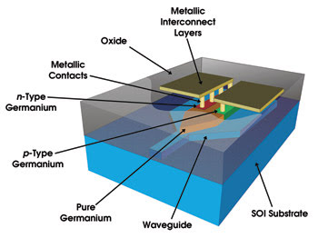
Figure 2. A depiction shows the various layers used in the manufacturing process of a germanium detector.
Infrared light is brought to the device input by a waveguide. The light heads straight for the absorbing germanium layer because of its much higher refractive index compared with that of silicon (4 vs. 3.5). Implants, both p- and n-types, define the junction, while standard metal connectors bring the electrical contact to the device. Using pure germanium can extend the spectral response of the devices to wavelengths as long as 1600 nm, where silicon-germanium absorption ceases.
We have fabricated a fully integrated, high-speed monolithic receiver using the process described in this article (Figure 3). Because it is possible to make all electrical and optical contacts necessary for testing before the 8-in. wafer is diced, defective die can be eliminated early in the production process.

Figure 3. This fully integrated receiver includes a photodetector, a transimpedance amplifier and a limiting amplifier.
Testing simplified
In a typical wafer-scale test, an optical beam at 1550 nm, modulated at 10 Gb/s, is coupled to the chip while high- and low-speed probes retrieve the receiver output and provide the biasing voltage and currents, respectively. A high-speed sampling oscilloscope records the receiver output in the form of an “eye diagram.” Figure 4 shows a typical eye diagram of the 10-Gb/s integrated germanium receiver output.
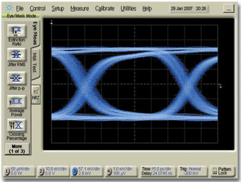
Figure 4. The typical 10-Gb/s eye diagram of the integrated germanium receiver output indicates high-quality transmission.
In this case, the germanium-on-silicon waveguide photodetector was biased at 0.3-V reverse bias, demonstrating the ability to operate at very low bias. This capability is particularly important for germanium-based photodetectors because, in general, they exhibit a much higher current leakage at a given voltage than do the corresponding III-V photodetectors.
Meet the authors
Cary Gunn is the co-founder and chief technology officer of Luxtera Inc. in Carlsbad, Calif,; e-mail: [email protected].
Gianlorenzo Masini is a senior principal scientist at the company; e-mail: [email protected].