Eric R. Mueller, Coherent Inc., and Yusaku Uehara and Kiyoshi Uchikawa, Precision Equipment Co., Nikon Corp.
Integrated circuits routinely produced by microlithography have feature sizes as small as 65 nm, well below the traditional diffraction limit for the exposure wavelength of 193 nm. Achieving this level of performance requires using a number of techniques to bypass the resolution limitations posed by the wave nature of light. It also means that the optical system always must perform to specification, with little tolerance for deviation. One problem in microlithography tools is uneven heating of the imaging lens elements by the excimer laser, which results in focus issues. This article explores the background and development of a CO2 laser-based system that controls lens heating and that has proved sufficiently robust for the demands of production semiconductor fabrication.
Wafer production relies predominantly on systems based on 193-nm excimer lasers to achieve feature sizes on the wafer as small as 65 nm. Current technology, albeit with certain refinements, already has proved capable of delivering feature sizes of 45 nm – and that may be extended to 32 and 22 nm over the next eight years or so.
The rules of geometrical optics state that the limiting resolution for an optical system is proportional to the wavelength of the light and the numerical aperture of the lens system. The result is that it is difficult to achieve feature sizes significantly smaller than the wavelength of light being used. How, then, can 193-nm lasers be used to produce features of 65 nm and below?
The answer is that microlithography uses physical – as opposed to geometrical – optical effects, such as phase and interference, to surpass the diffraction limit. Together these methods are called resolution enhancement technologies (RETs). Chemical processing techniques that can make a final feature smaller than the exposed area of the resist also are used.
One type of RET, dipole illumination, is useful when imaging reticle patterns in which most or all of the critical features occur in a single orientation; e.g., horizontal or vertical. In this technique, the reticle is illuminated from two off-axis angles. Interference between the zero and first diffracted orders then produces the necessary feature sizes in the focused patterns for the preferred orientation, while still delivering sufficient resolution in the orthogonal orientation.
The off-axis dipole illumination results in a very nonuniform intensity distribution at the pupil of the projection lens, however. Because there is some small amount of light absorption in the lens elements, they become heated by this absorption. This uneven heating results in astigmatism in the final focused image. Astigmatism produces a separation between the best focus position for horizontal and vertical lines in the pattern, degrading the ability of the system to simultaneously image horizontal and vertical features.
Infrared aberration control
Nikon’s solution to heating-induced astigmatism is to use a CO2 laser to selectively heat one of the projection lens elements in a way that cancels out the effects of excimer laser absorption. It is useful under dipole illumination conditions as well as in any other situation that creates nonuniform heating in the stepper lens.
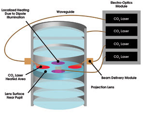
Figure 1. In this simplified representation of the infrared aberration control, two of the four lasers are actively heating the lens surface.
Figure 1 illustrates an extremely simplified schematic of the process. The output from each of four CO2 lasers is led through a flexible hollow waveguide to a beam delivery system near the stepper lens. After conditioning in the beam delivery system, the final output is delivered to the stepper lens surface through a rigid hollow waveguide. Strong absorption of the infrared light by the lens results in rapid, highly localized heating.
Figure 2 shows the major functional components of the optical system. The electro-optic module contains four lasers (only one is shown for clarity), and the output of each is monitored by a thermopile-based power sensor. The sensors provide a continuous reading of the health and status of the laser source and show how much power is being launched into the flexible waveguides.
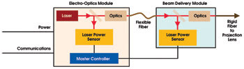
Figure 2. This block diagram shows the electro-optics and beam delivery modules in the IAC.
The waveguides lead to four separate beam delivery modules, each containing a thin-film polarizer, a power sensor and optics to launch the beam into the rigid waveguide, which is part of the stepper lens assembly produced by Nikon. Polarized light is sent to the lens because using only the p-polarization orientation minimizes reflectance, producing higher absorption at the lens surface. By comparing the power readings in the beam delivery modules with those from the electro-optic module, the system can determine the transmission efficiencies of the flexible waveguides and can signal whether alignment or other problems are present.
An embedded microprocessor monitors and controls all laser functions as well as those from the detectors. It also manages all the internal control loops; i.e., digital loops using an occasional proportional and differential feedback architecture.
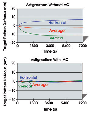
Figure 3. Astigmatism in the focal plane of the projection lens is shown without and with IAC.
Figure 3 quantifies the benefits of the infrared aberration control (IAC) system. The first graph shows that lens heating after just a few minutes of dipole illumination produces an astigmatism of nearly 20 μm in the focal plane. The second shows that the astigmatism is virtually eliminated when the IAC system is engaged.1,2,3
System development issues
Coherent Inc., which designed and built the IAC subsystem, faced several significant challenges during the development process because of Nikon’s stringent performance, packaging and delivery requirements. For example, the first prototype of the beam delivery was needed just three months after the development agreement was signed, and a beta test unit of the entire system, including software, was delivered after only nine months.
The largest technical hurdle was posed by the very large dynamic range over which the IAC must operate, which leads to numerous optical, performance and thermal challenges. First, the Nikon specification requires that the IAC deliver from 0.1 to 250 mW from the beam delivery module, with the ability to set the power to a precision and accuracy of 0.1 mW over the entire range.
To meet Nikon’s schedule, Coherent engineers built the system around a standard 30-W, air-cooled CO2 laser – Model C-30 – designed for marking and materials processing applications. The C-30 was chosen because it provides good transverse mode quality, a high dynamic range and excellent output stability. This approach reduces cost because it uses a product that already is being manufactured in volume, and it also increases reliability because the C-30 is well-proven and characterized.
However, the standard C-30 is designed for optimal operation – in terms of efficiency, noise, pointing stability and mode characteristics – at or near its maximum output power. This is because a typical materials processing customer purchases a C-30 to get 30 W of output and is unlikely to want to run the laser at just a few milliwatts.
A simple way to reduce the average power is to lower the pulse repetition rate. However, one of Nikon’s requirements is that the delivered power be updatable at a 10-Hz rate. It is necessary to run the laser at least 10 times faster than this rate (100-Hz minimum) to accomplish this. The required low-end output cannot be reached at repetition rates this high, so an operating repetition rate of 153 Hz was chosen, which delivers the necessary dynamic control and is also a prime number.
Using a prime number eliminates the chance that any intermodulation in the electronics – especially with 50- or 60-Hz noise from the power supplies – will occur at frequencies low enough to be problematic.
The output power problem was solved by using a special gas fill to deliberately skew the performance curve of the C-30 to lower powers. By utilizing a custom gas mixture and pressure, which alters the gain and saturation intensity characteristics of the laser, the stable operating range of the C-30 was extended down to 0.125 mW. The result is that the IAC uses a totally standard laser in terms of construction, with almost no incremental increase in cost for the special gas fill.
Another challenge was packaging-related. The optical alignment must be maintained over the entire operating range, even though the thermal loading changes dramatically over a 2500:1 power ratio. The problem is exacerbated by the extremely small package size; the electro-optics module is only 348 × 499 × 200 mm, and the beam delivery module is only 78 × 50 × 50 mm. This scale makes it difficult to adequately dissipate and remove waste heat. Extensive modeling of the packaging was performed using finite element analysis to refine the final design and achieve performance targets.
Ultimately, it was found necessary to thermally and mechanically isolate the cover over the baseplate on which the optics are mounted within the electro-optics module. Doing this eliminated a thermal pathway that otherwise would allow energy to transfer into the baseplate.
Figure 4 shows the displacement from the nominal position when all lasers are powered on full; the first part shows the starting design form, in which the cover was not independently mounted, and the second shows the improvement attained with independent mounting. The lasers are connected to the assembly by their front faces, which sit in a kinematic mount, enabling flexing along the axis of the laser, so that thermal expansion has negligible effect on system alignment.
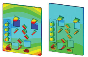
Figure 4. Depicted is a false-color map of displacement from the nominal position when all lasers are powered on full and the baseplate is not independently mounted and when it is independently mounted. Larger displacements are red.
The large dynamic range of the system also created electronic design challenges. In particular, noise can affect the analog signals in the power-sensing circuits when measuring very low light levels. For this reason, all electronic signals are digitized at their source; i.e., no analog signals are moved out of, or between, the electro-optics and beam delivery modules.
In conclusion, lasers have been a critical enabling technology in microlithography, providing a source of deep-ultraviolet light that has powered the move to ever-smaller circuit features. Now, the newest generation of microlithography tools use the infrared CO2 laser to take this even further, enabling sophisticated RETs to be used to their fullest extent.
Meet the authors
Eric R. Mueller is director of engineering at Coherent Inc., and Yusaku Uehara is a systems designer and Kiyoshi Uchikawa, a manager, both in the Optical Design Department of Nikon Corp.’s Precision Equipment Co.; e-mail: [email protected].
References
1. A. Hazelton et al (October 2007). Immersion lithography in mass production: Latest results for Nikon immersion exposure tools. Sematech Immersion Symposium.
2. T. Nakashima et al (2008). Thermal aberration control in projection lens. Proc. SPIE, CD, Vol. 6924, 69241V-1 to 69241V-9.
3. H. Magoon et al (May 1, 2008). Thermal aberration control. Microlithography World, online, Vol. 17, Issue 2.
Back from the Dead
When it comes to fabricating chips, lasers perform more functions than just lithography. When chips die, semiconductor makers bring them back to life, resurrecting them with lasers to cut the cost of computer memory.
That’s just one instance of a nonlithographic laser application relevant to semiconductor fabrication. Manufacturers also employ lasers to monitor chip-killing particulates and, increasingly, to dice pizza-size wafers into hundreds or thousands of chips. Memory chip repair has been practiced for several semiconductor generations, noted Martin Igarashi, director of the semiconductor products group at ESI, based in Portland, Ore. “We’ve been in the business for a long time – at least 20 years.”
A memory chip is arranged in rows and columns. Manufacturers build in a few extra rows that can be electrically swapped in, if needed. After the chip is fabricated, testing reveals any dead die and the nature of any defects. In faulty chips that can be repaired, laser-based systems zap the appropriate fuses, replacing a bad row with a good spare.
Targeting productivity
One memory repair trend targets improved productivity, which ESI achieves through a parallel technique. “We use a dual laser beam system. That is to improve the throughput,” said Igarashi.
Another trend, he noted, is toward smaller fuse banks that favor ultraviolet lasers instead of the currently standard infrared. However, ultraviolet damages silicon more than infrared does, so careful management of the beam is necessary.
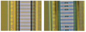
An example of an intact metal fuse is seen at left; an open one is on the right. Courtesy of ESI.
Lasers also have found a home in particle counting – a necessity because particulates measuring more than half the minimum-size feature can kill a circuit. Today, that means particles as small as 30 nm or so must be accounted for. For that function, manufacturers use counters consisting of a laser and a detector, which track the number of particles and their size by measuring scattered light.
Manufacturers employ a web of counters to automatically monitor airborne particulates at many points continuously. That places a premium on certain characteristics. “Laser diode reliability is absolutely the number one concern,” said Bill Shade, vice president of marketing and engineering at particle counter maker Lighthouse Worldwide Solutions of Fremont, Calif.
The company uses telecom-grade laser diodes that operate in the near-infrared at about 800 nm. Shade would like to see single-mode diodes with higher power. The power ups the signal, while single-mode operation enables diffraction-limited focus, a key requirement.
Finally, lasers increasingly are being used for dicing a wafer into individual chips. In July, ESI debuted a green picosecond pulsed laser system for this purpose. ESI’s Igarashi touts the advantage of the resulting cold ablation process, saying it creates less debris and causes less damage than a hot approach.
Based in Jena, Germany, Jenoptik has its own singulation solution, which uses a laser for heat and an aerosol jet for cooling. Uwe Wagner, head of global photovoltaic and semiconductor sales for Jenoptik, noted that the jet and laser produce forces that transform a surface dislocation into a total cleavage of the material.
The system won an award for innovation at this year’s Semicon West show, but improvements are planned, said Wagner. One is the use of a dry cooling jet. Another is the creation of the initial dislocation through laser-induced plastic deformation, which should increase throughput.
The current system uses a 1080-nm continuous-wave source, but that may have to be changed for other materials. “Near-infrared is fine for silicon, but it doesn’t work on ceramic, for instance,” Wagner said.
Hank Hogan, [email protected]
How It Works
An integrated circuit (IC) consists of numerous electronic components constructed on a single, monolithic semiconductor wafer. The detailed structure of these devices is built up layer by layer in a process called microlithography.
The first step is to coat a semiconductor wafer with a light-sensitive photoresist. This surface is then exposed to UV laser light that has passed through a reticle (mask) containing the desired circuit pattern. The exposed resist is developed and the wafer chemically etched to physically remove material from the exposed areas, thus producing the actual features on the wafer. The process is repeated many times on each wafer.