Photonic applications using the II-VI semiconductor zinc oxide (ZnO) are becoming increasingly prevalent, and research into even more uses is exploding, with hundreds of labs looking into the material’s unique properties.
ZnO has many properties that make it attractive for optoelectronic applications. It has a bandgap of 3.37 eV – the same as gallium nitride (GaN) – and an excitation binding energy of about 60 meV. It is transparent under visible wavelengths of light yet opaque under ultraviolet, making it a great UV sensor material. And it offers both piezoelectric and pyroelectric characteristics.
However, what is really attractive about ZnO compared with GaN and other semiconductors, such as cadmium selenide, is that it is environmentally benign. Semiconductor manufacturers are feeling increased pressure to include nontoxic materials in their products.
Such materials are easier to recycle, and outright biocompatibility of ZnO makes it a promising candidate for optoelectrical medical devices that can be inserted into the body.
Another intriguing aspect of ZnO crystals is that they readily form specific shapes, depending on the method used to create them. Each shape results in a slightly different set of photonic, piezoelectric and mechanical characteristics.
“ZnO with various shapes, including nanowires, nanorings, nanorods, nanobelts, nanotubules, nanohelixes and so on, have been synthesized by various methods and studied in the past decade,” said Wei Zhong of the Nanjing National Laboratory of Microstructures in China. “As a result, the properties of ZnO were found to depend on the shape and corresponding synthesis method.”
Thus far, however, bandgap tunability seems to depend more on changing the size of the crystal than on changing its shape.
Crystal formation
Typically, ZnO crystals are fabricated through thermal evaporation, chemical vapor deposition (CVD), metallorganic CVD, pulsed-laser deposition or template-based growth techniques. Unfortunately, all of these methods are used at a steep cost in time and money. High temperatures or vacuum typically are required, along with complicated processing steps and, often, noxious chemical compounds.
“In other words,” Zhong said, “the methods aren’t suitable for large-scale production [at] low cost.”
Zhong’s group currently is testing novel and less toxic fabrication methods that would produce doped ZnO microcrystals more simply and cheaply. The team’s focus is on using transition metals such as manganese, cobalt and iron to dope ZnO nanorods for use in nanoscale magnetic data storage media.
But Zhong and his colleagues aren’t the only ones intrigued by the possibilities of ZnO.
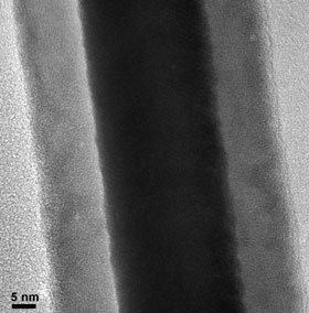
“ZnO demonstrates an extremely diverse range of tunable geometries, from dots to rods to wires to tri- and tetrapod motifs,” said Jeffery L. Coffer, chemistry professor at Texas Christian University in Fort Worth. He and his colleagues recently published work on the latter form – four-pointed objects with shapes like children’s jacks – which emit two distinct wavelengths after being coated with erbium ions and irradiated. They also found that adding a layer of germanium prior to erbium doping enhanced the tetrapod’s photoluminescence. Their report appeared in the Jan. 6, 2010 issue of Crystal Growth & Design.
Zinc oxide can be used to add features to a variety of nano-meter-scale structures. Shown is a germanium-core nanowire coated with a shell composed of erbium-doped ZnO. Courtesy of Jeffery L. Coffer, Texas Christian University.
“We are currently attempting to construct core/shell platforms that combine the properties of reactive nanoscale semiconductors such as germanium that can be packaged and passivated with the stable ZnO shell, both with and without additional dopant species,” Coffer said. “It is a rich field with plenty of things to explore.”
Along with changes in morphology, doping adds character to ZnO crystals. Doped with erbium, for example, ZnO emits at 1.54 µm and is particularly useful in LEDs, laser diodes and optical amplifiers. Upconversion permits emission in the visible range. Other common dopants include aluminum and indium.
Laying them down
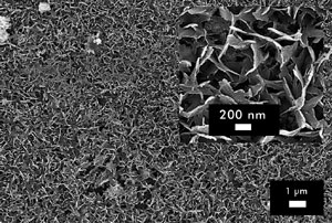
Another key to effective use of ZnO in optoelectrical or optomechanical devices is finding the best substrate upon which to grow or deposit the crystals. According to Eric Prouzet and his colleague Kam Tong Leung, both from the University of Waterloo in Ontario, Canada, there remain challenges in devising inexpensive conductive substrates. They also note that developing novel ways to create specific micro- or nanoscale patterns of ZnO on a substrate is of high importance.
A scanning electron micrograph shows zinc oxide crystals grown on a thin film of polypyrrole. Courtesy of Eric Prouzet, University of Waterloo.
“The challenge is to achieve large-scale preparation on cheap supports like plastic films as well as integration [into] specific devices,” Prouzet said.
Prouzet, Leung and their colleagues reported in the Jan. 12, 2010 issue of the journal Chemistry of Materials on one such candidate substrate, polypyrrole. A fairly well-known conducting polymer, it can be formed into wide swaths of thin film that are conductive enough to permit growth of ZnO nanocrystals via electrodeposition.
Because it is transparent to visible light yet darkens when exposed to ultraviolet wavelengths, ZnO also can be used as the basis of UV sensors. Rohm Semiconductors USA LLC, based in San Diego, recently announced what it calls a high-precision UV sensor that comprises a ZnO thin film. The device is sensitive enough to distinguish between the UVA (320 to 400 nm) and UVB (280 to 320 nm) bands without the use of an optical filter.