Since the notion of slow light first became
a reality more than a decade ago, scientists have been exploring its use in fundamental
studies of light-atom systems as well as for long-term applications in all-optical
data processing, quantum communication and sensors.
When light is slowed down, it is forced to interact more strongly
with the confining material. This is key to devices in sensing, quantum information
and all-optical signal processing for optical communication. There has been recent
progress in exploiting slow light for nonlinear signal processing, such as to demonstrate
enhanced four-wave mixing, and in observing striking nonlinearities, including third-harmonic
generation in silicon.
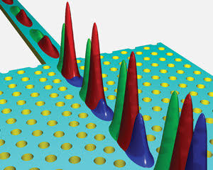
This picture illustrates four-wave mixing, a key nonlinear process
that is enhanced by slow light. Courtesy of the University of St. Andrews.
“The field has been studied theoretically for about 100
years; however, it wasn’t until 1999, when [Zachary] Dutton, [Stephen E.]
Harris and [Lene Vestergaard] Hau demonstrated slow light in a BEC [Bose-Einstein
condensate], that it became popular,” said professor John C. Howell of the
University of Rochester in New York. “The reason for the popularity was the
magnitude of the slowing. When we think about the absurdity of the speed of light
– 300 million meters per second – it is difficult to wrap one’s
brain around. However, they were able to slow a pulse of light down to about 17
m/s, albeit only for about 100 µm of propagation distance.”
As news of the accomplishment spread, a new field of optics was
born. For the first time, light was transformed to a speed in the realm of human
comprehension. The race then was on to see which materials provided the best slow-down
capability.
Slow light can be achieved by using material resonances; for example,
via electromagnetically induced transparency or stimulated scattering effects such
as Brillouin or Raman. Recently, some studies have indicated that stimulated Brillouin
scattering in silica optical fibers may not provide the desired enhanced light-matter
interaction.
A more promising approach, perhaps, is to slow down light using
the resonances created by microstructures such as Bragg gratings and photonic crystals.
This type of enhancement is similar to that provided by resonant cavities. Importantly,
it offers enhancement over a large bandwidth, enabling slow-light waveguides to
process high-bandwidth signals.
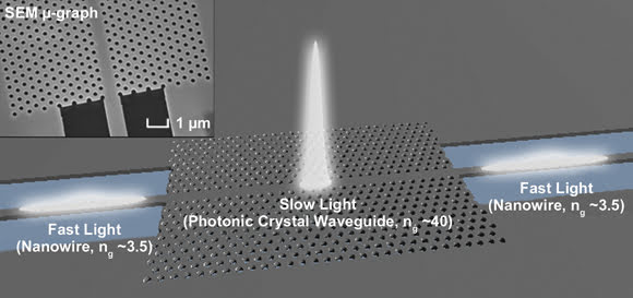
Schematic of slow-light propagation of pulses in a photonic crystal waveguide. Energy density
of pulses in the slow mode is increased and, along with distributed feedback effects,
enhances interactions with the material of the photonic crystal waveguide. (Inset)
Scanning electron microscopy micrograph of a nanowire coupled to a silicon photonic
crystal waveguide. Courtesy of the University of Sydney.
On April 12, 2010, Optics Express published a paper detailing
a major advance in photonic crystal engineering that enabled a record sixteenfold
increase in processing speed for a silicon device. The authors believe that this
improvement has opened the door for slow light to play a key role in ultrahigh-bandwidth
telecommunications systems.
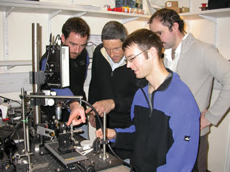
Professor Thomas F. Krauss and his team look at slow-light samples on the optical setup. Courtesy
of the University of St. Andrews.
Professor Benjamin J. Eggleton, co-author of the paper, is a pioneering
scientist in harnessing slow light for telecommunications systems and is director
of the Centre for Ultra-high Bandwidth Devices for Optical Systems ARC Centre of
Excellence at the University of Sydney in New South Wales, Australia.
“The goal of all photonics researchers is to control the
flow of light,” Eggleton said. “Currently, we have tools to control
the direction light moves in, and the next big challenge is controlling the speed
of light. If we can slow light down, then we have another degree of freedom that
we can use to control light.”
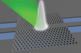
Green-light emission as seen by the naked eye. The green light is created from C-band IR light
through third-harmonic generation, occurring here in a silicon photonic crystal
chip. The red stages are for fiber coupling to the device. Courtesy of the University
of Sydney.
The photonic crystal structure used by Eggleton and his colleagues
was designed and fabricated by researchers at the University of St. Andrews in the
UK, led by professor Thomas F. Krauss. Their special dispersion engineering technique
led to broadband slow light, breaking a fundamental barrier in using slow light
to effect high-bandwidth signals. The team successfully demonstrated a propagation
of 640-Gb/s signals through a photonic crystal chip.
In an earlier example of slow-light-enhanced nonlinearities in
photonic crystal structures, the Sydney and St. Andrews researchers reported the
observation of green-light emission via third-harmonic generation. As reported online
in Nature Photonics on March 22, 2009, green light is ejected out of a slow-light
silicon photonic crystal structure, which can be observed easily with the human
eye.
Schematic of green third-harmonic emission from a broadband IR pulse
in a photonic crystal waveguide. The emission of the green light is mediated by
the photonic crystal and directed in certain angles as dictated by phase matching.
Courtesy of the University of Sydney.
“As well as being of fundamental significance, this scheme
offers a very elegant and compact method for monitoring transmission impairments
on optical data streams simply by placing a low-cost, slow detector on the silicon
chip,” Eggleton said.
Slow light optical buffers
When slow light first captured the imagination of scientists in
1999, research was geared toward optical buffering. Optical buffers are a key component
to overcoming data packet contentions in switches and routers.
Suppose two signals on two different lines must be routed to the
same output line. If they arrive at the same time, either one or both of the packets
will be rejected. If one of the optical packets could be slowed down until the other
packet has been successfully put on the line, then both signals could make it onto
the appropriate output line.
“Currently, optical buffers require conversion to electrical
signals, computer buffering and then reconversion to optical signals,” Howell
explained. “From a bottom line, one wishes to reduce the size, power and cost
requirements of the buffers needed to perform this task.”
It turns out, however, that slow light buffering is very hard
to achieve, whereas electronics already takes care of this very well. “There
have been a number of impressive demonstrations [of slow-light buffering], but they
are either incompatible with integration or have other practical limitations,”
Eggleton said.
Going one step further and stopping light is a key pursuit for
the quantum information processing community. Stopping and storing light is one
of the holy grails of photonics and will enable future on-chip, all-optical memories.
For Krauss, professor of optoelectronics at the University of
St. Andrews, all-optical memories will not be able to compete with gigabit-size
electronic memories. Instead, he envisages future optical buses on multiprocessor
chips requiring the storage of a few bits of information to avoid contention between
processors.
In more fundamental studies, metamaterials are creating excitement
as a new platform for photonics. Metamaterials may have a negative refractive index,
which means that they can be arranged to slow down and stop light in its tracks
by reversing the direction of its phase.
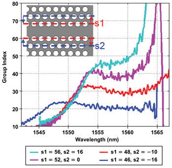
Group index change, with wavelength for dispersion-engineered photonic crystal waveguides, was
produced by the Krauss group at the University of St. Andrews. The ‘s’
values are shifts off the photonic crystal lattice of rows of holes in nanometers.
In this case, the lattice period is ~410 nm. The image was reproduced from Monat
et al (January 2010), IEEE J. Selected Topics in Quantum Electronics, Vol.
16, No. 1, p. 334.
Scientists such as Ortwin Hess, professor and Leverhulme chair
in metamaterials at Imperial College London, are investigating the physics of stopped
light and advancing the science that may lead to the much-publicized invisibility
cloak.
At this stage, achieving the shielding ability of Harry Potter’s
cloak remains a theory, but Hess recently met with Andrea Di Falco at St. Andrews
to discuss a recently demonstrated flexible metamaterial that could become a building
block for an invisibility cloak.
Much of today’s slow-light research lies in enhancing light-matter
interactions. Apart from the potential for all-optical signal processing, enhanced
light-matter interactions could boost the efficiency of nanolasers, frequency conversion
schemes, quantum information systems and sensors. One issue with using slow light
in sensing applications, however, is finding a low-cost solution.
Currently at a loss
The biggest challenge facing today’s slow-light community
is overcoming the limitation of loss. Losses go hand in hand with slowing light:
As light-matter interactions are enhanced, so, too, are losses. In particular, losses
in photonic crystals can increase significantly with reduced velocity, limiting
the applications of such waveguides in all-optical devices.
“Most applications are now limited by losses in the slow-light
regime,” Krauss said. “Even though our understanding of the nature of
losses has improved dramatically and already resulted in substantial improvements
that have led to the nonlinear results mentioned above, more needs to be done.”
However, Eggleton points to recent studies in fabrication-induced
propagation losses conducted at St. Andrews that hint at methods that may be able
to reduce losses associated with slow modes.
A problem that threatens slow-light research in the US concerns
another type of loss: funding. For the past five years, DARPA has provided strong
support for slow-light research, but Howell believes that this could be coming to
an end. “The European community is really the only group that is getting significant
funding. I think it will mostly die out in the US, unless some new initiative comes
through or unless there is another big ‘breakthrough’ that captures
the attention of the broader public again.”
It is always difficult to predict when the next leap in technology
will take place. The most tangible applications may be in biosensors, where the
enhanced-light-matter interaction provided by slowing down the light may result
in exquisitely sensitive devices, which Krauss estimates could become prototypes
in three to five years.
Although current state-of-the-art results have been achieved in
photonic crystal structures, these have typically been fabricated using electron-beam-lithography
processes. The drawback is that these methods do not scale easily to low-cost production.
Advanced photolithography or nanoimprint lithography could offer a solution, Eggleton
said.
“High-end applications in quantum information might provide
a niche without too much advancement in fabrication technology,” he added.
“Applications in sensing and communications are likely to require cheap methods
of mass production before slow light can make an impact.”