Micro-LED displays offer performance advantages over legacy technologies for product innovations, such as smartwatches and tracker bands. Yet, mass production remains elusive.
JAMES SCHLETT, CONTRIBUTING EDITOR
Last fall, Samsung Electronics’ visual display business vice president, Tae-yong Son,
described the company’s
process for manufacturing micro-LED displays as
“Trying to place a tiny object, smaller than a human hair, in a specific position and angle.”

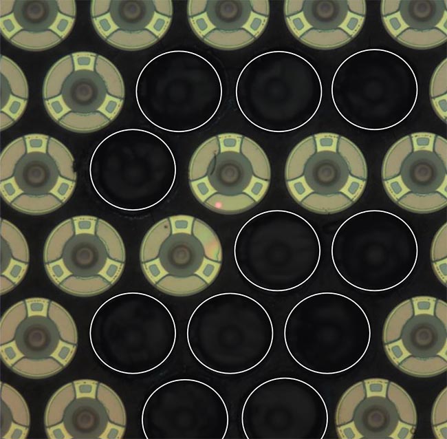
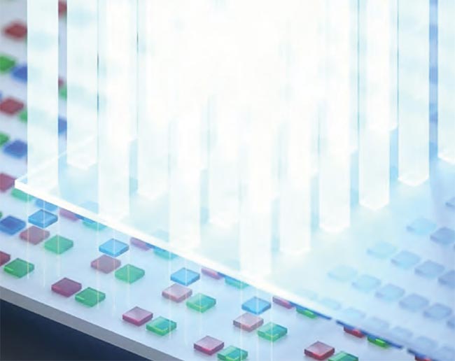
Micro-LED displays range in size from large-area TVs to smartwatches. In addition to size varieties, the numerous manufacturing processes available to display makers means that the industry remains in search of a clear path to sustainable mass production practices. Courtesy of Samsung Electronics.
“Then, repeat this action over half a million times,” Son said.
Step one is a major technical undertaking; it is hardly as formidable as those posed by steps two to 500,000.
Manufacturing challenges, such as
precision placement and process repeatability, which are necessary to ensure optimal performance in final systems,
are a core driver of the high cost of micro-LEDs that are currently under development. Samsung, for example, has priced its 4K 146-in. “Wall” display offering at $219,999.
Further, Samsung said, on top of transferring 510,000 sub-50-µm micro-LEDs from a wafer onto a substrate, the fabrication and assembly phases precede an additional 600 h of reliability testing and stabilization measurements.
The laser trimming process (shown) as well as a cleaning process are deployed as part of the fluidic self-assembly (FSA) method to remove defective micro-LEDs from the carrier substrate before the micro-LEDs are harvested. Courtesy of eLux.
Hitting process walls
Fabrication challenges have a direct tie to low production capacity. This is part of a troubling equation that the micro-LED industry is striving to rework.
Consider the notion of mass production
— a concept that is fundamental to a technology’s commercial success. Paul Schuele, CTO of Vancouver, Washington-based eLux, says that for larger-sized micro-LEDs, such as TVs and monitors, mass production means producing 500 86-in. displays per month.
Although the use of laser transfer technologies, including the ones at Samsung, gives photonics an edge in the race to micro-LED mass production, other major players in this arena, such as LG and Apple, are exploring non-photonic manufacturing methods, such as electrostatic transfer. Another commonly used technique, fluidic self-assembly (FSA), falls on the periphery of photonics.
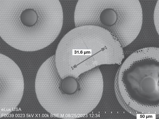
The laser trimming mechanism may introduce new defects to a micro-LED under development, including fragments and solder residue. Courtesy of eLux.
For the industry to move toward reaching mass production levels, and for photonics to remain dominant, materials and processing strategies must be optimized, and inspection speeds must be accelerated.
“The industry is well below mass production levels, and we have reached the point where most of the R&D and demo labs have reached diminishing returns at the volumes being run,” Schuele said.
“So, mass production is required to drive down costs to the point where mass production makes economic sense. Kind of a chicken-and-egg paradox.”
Until this happens, price points for micro-LED technology are apt to remain prohibitive for consumers. This factor also slots into the present-day micro-LED equation.
For its part, the MicroLED Industry Association (MIA) does not anticipate that its members will achieve mass
production — however it is gauged —
for almost all applications for two to five years. In this period, drastic changes will be required in several micro-LED manufacturing processes, especially in epitaxial wafer (epiwafer) growth, chip processing, and transfer. Though micro-LED displays offer performance advantages in brightness, efficiency, and lifetime, their production costs remain considerably higher than their liquid
crystal display and OLED counterparts.
This is why the MIA regards that the demand for micro-LEDs is largely driven by such high-end applications as Samsung’s Walls. A lack of demand for more established, and cheaper, applications is another industry-wide consideration.
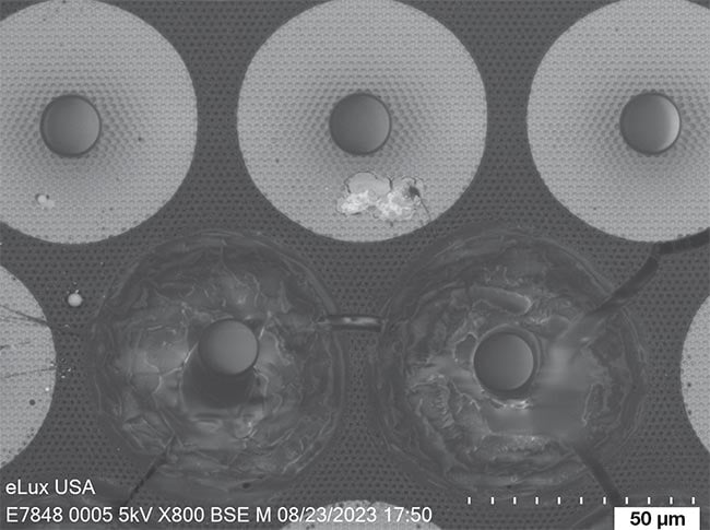
For micro-LED developer eLux, trimming process challenges are caused by the laser spot size being larger than the target micro-LED diameter. Courtesy of eLux.
“For mass markets, such as smartphones, IT displays, [and] consumer TVs, it will be very challenging for micro-LED displays to be adopted as it’s not likely consumers will accept very high costs, and the advantages of micro-LEDs over OLEDs are not as prominent,” said Ron Mertens, MIA managing director.
Open playing field
In December 2023, the MIA released a state-of-the-industry report and future roadmap in which the association said, “It is plausible that as the micro-LED industry matures, different companies will still choose various technologies and architectures, and it is also possible that displays meant for different applications will be different in terms of manufacturing and architecture.”
Mertens anticipates that a first wave of micro-LED displays will be produced at low-volume settings using current transfer processes. “For real mass production at competitive costs, there will need to be a real change in transfer processes,” Mertens said, with an eye toward the critical two-to-five-year period that the MIA believes will be the mass production window for micro-LED producers globally. By this time, he expects that industry will be much more prolific in its use of processes.
This would be a deviation from current practices. Most industry players use the same process(es) to make OLEDS, for example.
According to Mertens, micro-LED makers will face an open playing field as a result, at least in terms of manufacturing approaches. Certain methods are more established than others. For displays that are the size of smartwatches and larger, for example, designers and manufacturers must include as many micro-LEDs as
possible on an epiwafer with a pixel pitch of ~60 µm, if not larger. Laser-based
approaches are favored by producers to help strike this balance.
Laser lift-off (LLO), which is often mentioned with another distinct process called laser-induced forward transfer (LIFT), is a mass transfer process that separates finished micro-LEDs from the growth wafer without damaging the micro-LED or the wafer. LLO is well established, and variations to the technique continue to distinguish it from other methods.
Laser manufacturer Coherent, for example, has demonstrated a laser solution to process individual micro-LEDs as small as 5 µm via both LLO and LIFT processes. Using a deep-ultraviolet (DUV) excimer laser, LLO transfers multiple micro-LEDs from the epiwafer with a single pulse, or temporary carrier. In contrast, with LIFT, the transfer usually involves the use of polymer-based adhesives to preassemble micro-LEDs on a temporary carrier wafer. Using the optimized material, which is transparent for a DUV laser, only the micro-LED will be transferred to the substrate without residues.
Consideration for residue and epitaxy are critical. “The epitaxy used in the LED impacts the wavelength needed for successful lift-off. As the bandgap of the epitaxy increases, higher photonic energy is required from the laser, i.e., shorter wavelengths for a lift-off process,” said Bill Kallgren, systems marketing manager for IPG Photonics.
In FSA, the laser adopts more of a complementary function. This method
involves the dispersion of micro-LEDs into a liquid. Eventually, in this process, the micro-LEDs are designed to land in wells that ultimately become the base of a substrate. The fluidic technique relies on laser trimming and cleaning processes to remove defective micro-LEDs from the carrier substrate before the micro-LEDs are harvested. The company eLux, for example, uses a 355-nm diode pumped solid-state laser at 50 kHz for this purpose.
“In particular, beam shaping to effectively deliver the right amount of power to the micro-LED center is critical,” Schuele said. According to Schuele, heating the underlying adhesive without exploding the LED is also critical. “Defocused, misaligned optics, and misalignment of the laser spot to the disk all cause unsuccessful repairs.”
FSA, like LLO and LIFT, remains the subject of investigative trialing. Last
summer, researchers from LG Electronics and Seoul National University demonstrated an agitation-based, surface-
tension-driven FSA technique to assemble a micro-LED lighting panel with more than 19,000 disk-shaped gallium nitride (GaN) chiplets1. The assemblage took
60 s, with each chiplet measuring 45 μm in diameter and 5 μm in thickness.
The demonstration followed similar
results previously achieved by eLux. Using an automated FSA tool, the
company fabricated a 12.3-in. micro-LED display of 518,400 GaN micro-LEDs in a period of 10 min. The demonstration display featured only 34 failing subpixels; all but one were repaired with a laser.
Today, Schuele said, eLux is focusing on the public information display market. The company’s goal is to enter into the sector with a display of 42 pixels per in. (ppi). Its 12-in. diagonal displays (480 × 180 at 42 ppi) use 460-nm GaN micro-LEDs with quantum dot color conversion for green and red. They are tiled to form large, bezel-free displays.
Looking ahead, eLux aims to increase its ppi values and hopes to ultimately achieve 800 to 900 ppi. FSA is not a viable method for augmented or virtual reality applications, for example, because of the tiny pixels that these applications demand.
“For automotive applications, like instrument clusters and center console displays, 300 dpi is probably sufficient, while the high brightness and long life are clear advantages over OLED technology,” Schuele said.
eLux is also moving from using LEDs with diameters of 50 µm to 25 µm.
Release and catch
In addition to upping its ppi value(s),
eLux plans to further downshift — from 25 µm to 5 µm LEDs. The laser trimming challenges that it faces may inhibit this transition. According to Schuele, a major challenge in the trimming process stems from the laser spot size being larger than its target micro-LED diameter, which is 25 µm.
Therefore, laser optics and beam alignment are crucial to prevent damage to neighboring micro-LEDs. Although Schuele said that <0.01% of laser trims generate new defects, the aim of the company’s “selective harvest” in-process quality assurance approach aims to decrease the value even further, down to 0%.
A manufacturing solution deployed at Coherent uses laser lift-off (LLO) (top) to reshape the ultraviolet laser beam. Then, laser-induced forward transfer (LIFT) changes the pitch of the selected micro-LEDs (bottom). Courtesy of Coherent.
As it relates to market presence and consumer adoption, micro-LEDs must shrink to the single-digit micron level, according to Oliver Haupt, director of strategic marketing for Coherent. This is vital to the technology ultimately overcoming the current cost advantages of legacy and competing technologies, including OLEDs.
“Today, the individual processing steps are too slow, or with a bad yield, and material costs are too high, as well. It will take some more time to get all that harmonized and standardized,” Haupt said. “It starts with the right backplane, the circuits, bonding materials, and, of course, with the quality [efficiency] of the micro-LEDs in all three colors.”
Blue and green micro-LEDs are grown on a sapphire wafer and, in the case of Coherent, LLO is used to transfer the micro-LEDs onto a temporary carrier. Red micro-LEDs are made on gallium arsenide wafers, from which they must be ground or etched away. After optimizing the micro-LEDs’ release and “flying” phase in the transfer process, Coherent and other industry players are working
to improve the “catch” phase. This
step necessitates the use of a bonding
material that is both sticky and soft enough to avoid damaging the finished micro-LEDs upon landing, according to Haupt.
Further, according to Kallgren, wafer bonding itself must be optimized.
“Requirements vary if there is a temporary bond to a handle wafer for downstream LIFT or if a micro-LED array is being directly bonded to a CMOS wafer,” he said.
Jayna Sheats, CTO of Silicon-Valley based Terecircuits, which specializes in materials for advanced manufacturing processes, said that one challenge associated with LIFT is the distribution of fragments resulting from the ablation of the sticky polymer on the temporary carrier. Terecircuits developed a photopolymer with high bonding strength that withstands temperatures >200 ºC. DUV irradiation can trigger its decomposition into completely volatile small-molecular weight fragments, resulting in low fluence and no residue.
Consequently, micro-LEDs yielded from the LIFT process land on the target substrate with uniform pressure. Because the approach uses a photochemical sensitization event, which is separate from polymer decomposition, there is less effect on neighboring regions, Sheats said. Also, there is a minimal, if any, heat-affected zone.
The method derives conceptually from photolithography.
“There is less to reinvent to get to a fully satisfactory production process than with methods that require both new tools and materials, and new process monitoring methods,” Sheats said. “The major limitation has been a material that can produce the desired transfers cleanly as well as at high throughput, which is where our innovation comes in.”
Uniformity
The need for production uniformity
presents challenges to mass production that extend beyond the challenges posed by the transfer process. Production
uniformity is measured by overall performance, physical makeup/composition,
and appearance.
“Because micro-LEDs are an emissive
display type (each pixel emits its own light) there can be wide variability in luminance [brightness] and chromaticity [color] from one pixel to the next, causing
an uneven appearance,” said Scott McLeod, director of product management and marketing at Radiant Vision Systems. This uneven appearance is called mura.
Producers test and inspect the micro-LEDs under development at several points on the manufacturing process timeline. For example, wafers must be inspected before transfer. The etching(s) on the
wafers, as well as the growth of the micro-LEDs, must also be evaluated
during the process.
“Micro-LED manufacturers are looking for a technology that can handle single-micron micro-LED sizes and
that can provide the highest speeds in electroluminescence (EL) wafer inspection,” said David Lewis, CEO of
Jerusalem-based InZiv. To improve
quality industry-wide, Lewis said, EL testing is needed at high speeds to look
for defects and irregularities on the smallest dies. InZiv’s solution, which the company introduced last year, is a high-resolution EL system created for the inspection of single-micron die sizes at speeds of 6 million LEDs per hour. It can also test both flip-chip and vertical chip configurations.
Tests and inspections occur at separate points in the process chain. Manufacturers may use photometric and/or colorimetric imaging systems after the transfer and bonding stages. The required performance parameters of these systems vary. Radiant Vision Systems, for example, markets imaging photometry and colorimetry
systems with high-resolution sensors of 45 MP, 61 MP, and 151 MP. To support
precise measurements of nanoscale elements in micro-LED and quantum dot displays, the systems also feature fractural pixel method algorithms and optical components with 5 to 10× and 20× microscope lenses.
“Micro-LEDs have driven a need for higher-resolution inspection systems and solutions capable of measuring at the
individual pixel and subpixel level,” McLeod said. “Accurate measurement typically requires a minimum of four
sensor pixels applied to capture the image of each display pixel.”
Reference
1. D. Lee et al. (2023). Fluidic self-assembly for MicroLED displays by controlled
viscosity. Nature, Vol. 619, No. 7971,
pp. 755-760.