Tripled Nd:YAG Fills Gap by Drilling Holes
Daniel C. McCarthy, News EditorLike everything else on microelectronic circuitry boards, the diameters of microvias are shrinking. Mechanical drilling methods, still the most common, are limited to creating hole diameters greater than 100 µm. But as designs begin to approach via diameters smaller than 75 µm, laser technology is carving a niche by producing smaller holes at faster speeds.
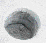
Electro Scientific's tripled Nd:YAG laser drilled this 100-µm blind via through an 18-µm copper layer a material highly reflective to CO2 laser wavelengths. Courtesy of Electro Scientific Industries Inc.
Companies such as PhotoMachining Inc. are capitalizing on the ability of lasers to solve an array of drilling problems for board manufacture. Most recently, the company added a tripled Nd:YAG laser system from Electro Scientific Industries Inc. to its range of drilling solutions.
According to CEO Ronald D. Schaeffer, PhotoMachining had based its micromachining services primarily on CO2 and excimer laser technology. These lasers can achieve microvias half the diameter of mechanically drilled holes and are also effective in removing dielectric material from circuit boards. But the 10-µm wavelength and comparatively low peak-power densities of CO2 lasers make them ineffective in drilling reflective metals such as aluminum, gold and, most significantly, copper.
"CO2 was very fast, but we had to pre-etch overlying copper, which slowed the overall process down," Schaeffer said. He added that excimer lasers could remove both dielectric layers and copper, but operated at slow processing speeds.
After research, Schaeffer became interested in Nd:YAG lasers and, specifically, Electro Scientific's device, which he said is one of the few tripled Nd:YAG laser systems on the market. Besides its 10-kHz speed, the laser's 355-nm wavelength allows PhotoMachining to drill 25-µm vias in both dielectric and copper materials. Processing speeds can approach 40 holes per second in an 18-µm-thick copper conductor with a 50-µm-thick dielectric layer.
As vias get smaller, the market for drilling them with lasers is projected to expand. "Right now there's more than 400 lasers in the world doing this sort of work -- most of them in Japan," Schaeffer said. "By the year 2002, we will need 3000 laser drilling systems just for portable phones.
LATEST NEWS
- 3D Holography Integrated Glasses Could Unlock Mixed Reality May 2, 2024
- Generative AI Achieves Superresolution with Minimal Tuning May 2, 2024
- AmeriCOM Adds President and CEO: People in the News: 5/1/24 May 1, 2024
- Machine Learning Pushes High-Power Lasing Limits May 1, 2024
- IPG Names Industry Veteran Mark Gitin CEO Apr 30, 2024
- 16th Biannual Optatec Conference Continues in Frankfurt Apr 30, 2024
- Celestial Surface Mapping Tech Combines Established Techniques Apr 30, 2024
- TSMC Partnerships Target Integrated Photonics Capabilities Apr 30, 2024