All-Photonic Circuits at Hand
Michael Van BelleNanovation Technologies Inc. has entered the testing phase of its development of a fully integrated optical circuit, a technology that promises to deliver faster, higher-capacity communications to the marketplace by the end of the year, in packages significantly smaller than today's electronic circuits.
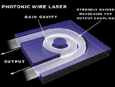
Nanovation's integrated optical circuit comprises a photonics ring laser, photonics switch and a strongly confined waveguide.
"We have the building blocks to create all-photonic circuits, and these circuits can be 100 times smaller and operate 100 times faster with greater efficiencies," said Bob Tatum, president and CEO of Nanovation.
The integrated optical circuits combine Nanovation's patented photonic ring lasers, photonic switches and strongly confined waveguides. The technology came out of Northwestern University's Transfer Technology Program, and the devices are being developed and tested at Nanovation's nanofabrication facilities on the university's campus in Evanston, Ill.
Similar to today's semiconductor integrated circuits (ICs), the photonic devices are planar, allowing them to be fabricated onto GaAs or InP semiconductor wafers, according to Roydn Jones, senior vice president for engineering.
Jones compares the situation with integrated optical circuits to the early days of semiconductor chips because of the ability to achieve a high level of integration. "Because of the size of devices and the ability to route photons [in waveguides with less than 5 µm radii], we could have thousands of devices on a single optical IC," he said.
The first patented device that enables this technology is the photonic ring laser, a circular waveguide etched on the substrate. When this ring is electrically or optically pumped, it emits laser light. Placing another planar waveguide close to the ring allows light to be coupled from the photonic ring. The output photonics can be routed to other optical devices just as electrons are routed with metal lines on conventional integrated circuits. "The optical IC is really very similar to die-on chips, but it uses photons instead of electrons," Jones said.
The second patented device is an optical resonator, which can switch light from one waveguide to another. Initial applications are in add/drop filters, multiplexers and demultiplexers, and high-speed optical switches for telecommunications applications such as wavelength division multiplexing (WDM) and dense WDM.
The technology will revolutionize several industries in the same way the transistor did years ago, Tatum said. "The transistor was a big deal, but this is even bigger. Photons run faster than electrons, and the circuits are smaller. They do not generate heat, and that eliminates any kind of electromechanical radiations -- there is no interference, in other words, with photons as there is with electrons."
Tatum expects potential licensees to be identified by the third quarter this year, with commercialization expected sometime in 2000.
LATEST NEWS
- Exail Signs LLNL Contract, Partners with Eelume Apr 26, 2024
- Menlo Moves U.S. HQ: Week in Brief: 4/26/2024 Apr 26, 2024
- Optofluidics Platform Keys Label-, Amplification-Free Rapid Diagnostic Tool Apr 25, 2024
- DUV Lasers Made with Nonlinear Crystals Enhance Lithography Performance Apr 25, 2024
- Teledyne e2v, Airy3D Collaborate on 3D Vision Solutions Apr 24, 2024
- One-Step Hologram Generation Speeds 3D Display Creation Apr 24, 2024
- Innovation Award Winners for Laser Technology Honored in Aachen Apr 23, 2024
- Intech 2024: AI Arrives on the Shop Floor Apr 22, 2024