A Growth Industry
Daniel C. McCarthy, Senior Editor
Photonic crystals are edging toward commercial application, thanks to advances in design, materials and manufacturing.
Photonic bandgap crystals serve as a microcosm of the photonics industry: Although microscopic
in structure, their versatility in manipulating photons could have a huge and pervasive
impact on nearly all optical components and instrumentation, enabling new generations
of tunable filters, low-loss waveguides, microlasers, all-optical switches and integrated
circuits.
The photonic bandgap these crystals create has
uses similar to an electronic bandgap, particularly if the crystal structure has
a carefully engineered flaw. The effect such flaws have on photons is analogous
to the effect dopants have on electrical current in a semiconductor: They open a
well-defined path, allowing bandgap photons to travel through the crystal. One
might argue that similar applications can be achieved through total internal reflection
— say, in a waveguide. But total internal reflection is inherently limited
by scattering losses at tight bends or small pointlike cavities. A bandgap crystal,
however, traps light so completely that it will direct photons around sharp bends
with little loss.
The lattice structure of a bandgap
crystal is on a scale with optical wavelengths and is based on alternating materials
with high and low dielectric constants. On a larger scale, similar periodic structures
can form bandgaps for microwaves, radio waves and even sound waves.
Whatever the scale, the principle underlying
how these crystals function is familiar to anyone who understands how a multiple-layer
thin-film filter uses interference to reflect specific wavelengths. Basically, the
lattice periodicity is spaced so that bandgap wavelengths destructively interfere,
thereby preventing their passage through the crystal. Constructive interference
enhances wavelengths outside the bandgap and allows them to propagate through the
crystal with little attenuation.
Thin-film filters and fiber Bragg gratings
fit the definition of one-dimensional photonic crystal structures. But they provide
only a one-dimensional bandgap that moves with a change in the angle of incidence
or other properties of the light. A multilayer film, for example, shows a bandgap
only for wavelengths propagating normal to the crystal. These types of structures
are simple enough to occur in nature. Hence, abalone shells’ iridescence derives
from the angular dependence of the bandgap frequency.
Although a partial bandgap in one dimension
is enough for filters and such, most of the potential and, therefore, most of the
interest in photonic crystals stem from two- and three-dimensional structures. Like
one-dimensional crystals, higher-order structures can filter selective wavelengths,
but in a like number of dimensions.
Trial and error
About 11 years ago, three-dimensional photonic
bandgap crystals existed only in theory. Like simpler structures, such as thin-film
filters, they promised to block photons within a certain wavelength band from propagating
through the crystal lattice. Unlike one- and two-dimensional crystals, however,
these structures would create a bandgap regardless of the direction the photons
traveled or their coherence, polarization or angle of incidence. The eventual application
of such structures was even more theoretical, but the main thrust was to do for
photons what semiconductors had done for electrons, and to progress from there.
Producing a structure that demonstrated
a functional optical bandgap proved difficult, requiring years of trial and error.
The earliest successes emerged in 1991 and borrowed from diamond’s tetrahedral
lattice. Shortly thereafter, face-centered cubic lattices of airholes in dielectric
appeared. These are actually extensions of the diamond lattice and, although they
have a smaller bandgap, they can be self-assembled. A third structure, modeled after
cubic scaffolding, produced an even smaller bandgap.
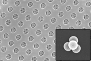
Self-assembled crystal fabrication has been limited to spherical colloids and,
therefore, to face-centered cubic lattices. But new colloids are emerging with
different shapes — including rods, ellipsoids and polygons — which
could enable lattices with wider bandgaps. Courtesy of the University of Washington.
Since then, researchers have modified
the lattice materials, components and shapes of photonic crystals, but the underlying
structures don’t stray far from the original three. Although new designs ease
fabrication or improve the bandgap, they still combine elements from both diamond
tetrahedral and face-centered cubic lattices.
Three-dimensional bandgap structures
can produce a complete bandgap, which offers plenty of application possibilities,
particularly if the light can be coaxed through a flaw in the crystal. By combining
such devices to control the propagation of light in predictable ways, researchers
could develop photonic integrated circuits, or if constructed from photosensitive
dielectrics, a crystal’s bandgap could be altered by incoming wavelengths,
thereby blocking or routing alternate wavelengths — making a photonic switch.
“You can guide light in a waveguide
or trap it in a cavity, but the next step is to combine them into devices,”
said Steven Johnson, a researcher at Massachusetts Institute of Technology in Cambridge.
“We have all these designs for things like channel drop filters, but they
haven’t been fabricated into three-dimensional systems except in the most
primitive sense.”
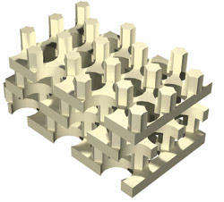
State-of-the-art designs for photonic crystal structures still borrow their
geometry from the decade-old diamond lattice configuration. The layers of the
structure shown here alternate dielectric rods in air and airholes in dielectric.
Courtesy of Massachusetts Institute of Technology.
Hence, integrating bandgap crystals
into a working device is a major goal, but Johnson said the research community is
still refining the essential building blocks.
“I don’t see any showstoppers,”
he said, in regard to integrated devices based on photonic bandgap crystals. “It’s
more a question of putting in the hours at this point. There are still some unknowns.”
Among those unknowns are how to fabricate
three-dimensional crystal structures in volume and how to invest them with functional
defects.
Stacked logs and marbles
It is no surprise that semiconductor fabrication
techniques would apply to the photonic analogue for semiconductor devices. About
five years ago, Shawn-Yu Lin at Sandia National Laboratories in Albuquerque,
N.M., used standard lithography techniques to create a crystal structure that resembled
a stack of logs. A derivative of the face-centered cubic lattice, Lin’s crystal
lattice comprised four layers, each with alternating rods and spaces laid in parallel
fashion.
He deposited, patterned and etched
the first layer as parallel silicon dioxide rods. He then filled the gaps with polycrystal line
silicon and polished the surface. After depositing a second layer of rods turned
90°, he applied the polymer again. Rods in the third layer ran parallel to
rods in the first, but they were located over the spaces in layer one. After a third
polymer application, Lin laid the fourth layer of rods, then etched away the polycrystalline
silicon, leaving a silica-and-air crystal lattice that had a complete three-dimensional
bandgap for wavelengths between 10 and 14.5 μm.
In the May 2 issue of Nature,
Lin described a similar structure that he made from tungsten, which showed a large
bandgap from 8 to 20 μm.
Besides being well-established and
understood, microlithography can produce complex features with enough accuracy to
engineer precise and functional defects in the crystal lattice. But few academic
laboratories have a lithographic stepper able to produce nanoscale defects. Consequently,
a number of researchers working independently have explored self-assembly methods
based on colloidal suspensions.
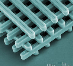
Microlithography can fabricate crystal lattices with complete three-dimensional
bandgaps, but it is both expensive in small volumes and not given to creating three-dimensional
defects. Courtesy of Sandia National Laboratories.
Early demonstrations showed that nanospheres
suspended in a meniscus align into orderly stacks as evaporation moves the meniscus
across a substrate. The stacked spheres serve as the mold for a photonic crystal
lattice: After a high-refractive-index material is injected between the nanospheres,
the spheres are chemically etched away.
This fabrication method is simpler,
faster and cheaper than lithography. And three-dimensional crystals are formed directly
on a substrate, which could prove handy in integrated optics applications. However,
if and when crystals become a growth business, so to speak, lithography’s
manufacturing benefits may win out.
“If this was something that Intel
was going to do, I think they would figure out how to do it with lithography,”
said Paul Braun, a professor of materials science and engineering at the University
of Illinois at Urbana-Champaign. “But from a research perspective, or in cases
where you need them in lower volumes, self-assembly makes more sense.”
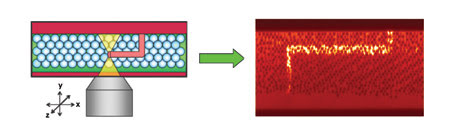
What’s the use of a three-dimensional bandgap if you can’t write
defects in three dimensions? One approach borrows the scanning method from
multiphoton microscopy to inscribe a three-dimensional defect through a bandgap
crystal. Courtesy of the University of Illinois.
Thanks in part to work by David Norris
and Yuri Vlasov at NEC’s Research Institute in Princeton, N.J., self-assembly
methods overcame early problems with unwanted defects and particle sizes limited
to 400-nm diameters. The small size, in particular, was a problem because it prevented
bandgaps in the potentially lucrative telecommunications window above 800 nm. Now
that unwanted flaws in the lattice are better controlled, the next challenge is
how to produce intentional defects to create waveguides and other devices.
Three-dimensional defects
Multiphoton polymerization is one approach, as
demonstrated by Braun and collaborators Wonmok Lee and Stephanie Pruzinsky. The
team injected a photosensitive monomer into the interstices of a colloidal template
and used a microscope objective to scan the focal point of an infrared laser through
the template’s interior. The intense light at the focal point polymerized
the monomer, allowing them to create three-dimensional waveguides in the crystal.
Defects demonstrated had minimum widths of 1.5 μm, edge resolution better than
100 nm and cut sharp curves with 500-nm radii.
Like Lin’s stack-of-logs structure,
self-assembled crystals define the size of their bandgap by the contrast between
the material components’ refractive indices — the greater the contrast,
the stronger the bandgap. Most self-assembled crystals aim for a contrast of at
least three; that is, a refractive index of 1 for air and an index of 3 for the
lattice material. But the multiphoton-generated defects in the University of Illinois
crystal are made of polymer, which has a refractive index of about 2.5. So the next
step for Braun and his collaborators is to find a way to etch out the polymer, leaving
an air guide embedded in the matrix.
That’s a challenge, because before
the polymer is etched out, a crystal lattice must be formed by depositing a high-refractive
material within the colloid template, and the polymer cannot easily withstand the
high temperature of most deposition processes. Braun said his group may have solved
this problem, but he refrained from revealing how until the solution undergoes
peer review.
It is possible, however, that he will
borrow from earlier work in which he deposited selenium in colloidal templates.
Selenium has a low surface tension, which allows it to easily penetrate the template,
a high refractive index and, most importantly, a lower melting point (217 °C).
Another limitation of self-assembled
crystals, as they stand today, is that they are stuck with a face-centered cubic
structure based on spheres. Forming tetrahedral lattices would deliver much larger
bandgaps, but such lattices require more complex colloidal structures that must
be oriented as well as organized within a structure. Spheres, unfortunately, do
not cooperate well and tend to collapse together like “marbles in a cup,”
Norris explained. But chemists at the University of Washington in Seattle are
working on a solution.
Led by Younan Xia, they innovated colloids
with different shapes, including rods, ellipsoids and polygons. Oddly, the most
complex colloids, the polygons, are also the simplest to form because they are essentially
extensions of commonly available nanospheres.
For example, Xia created polystyrene
tetrahedrons by confining an aqueous dispersion of monodisperse polymer spheres
in a cell. By slowly draining the liquid through the cell, the dispersion left spherical
colloids in notches along the cell wall. By controlling the ratio between the dimensions
of these holes and the diameter of the beads, he could produce well-defined nonspherical
clusters with consistent dimensions ranging from 150 nm to 5 μm.
The next step is to find a way to organize
these building blocks into a bandgap structure. One approach that Xia is considering
borrows from self-assembly methods and orients the colloids with either a magnetic
or an electrical field. Whatever the approach, he said, “It’s going
to be much more challenging than spheres.”
Holey logic
The relative ease in calculating in-plane bandgaps
helps explain why most of the early theoretical work was done on three-dimensional
photonic crystals. But, as Philip Russell pointed out, “A photonic crystal
doesn’t have to have a photonic bandgap to be useful. The bandgap is just
one feature.”
A case in point, as demonstrated by
Russell and a handful of other scientists, is photonic crystal fiber, which comprises
a one- or two-dimensional bandgap structure with a cavity that is kilometers in
length — or depth, depending on how you look at it. The cavity serves as the
fiber core.
Russell, a professor at Bath University
in the UK and chief technology officer for Blaze Photonics, also in Bath, pioneered
the development of hollow-core fibers. Fibers with similar configurations have sprung
up at Corning Inc. in Corning, N.Y., and OmniGuide Communications in Cambridge,
Mass.
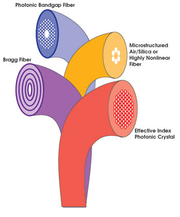
Only constructive scattering from a photonic
bandgap structure can guide light down hollow-core fibers, such as those facing
left. Other photonic crystal fibers use a modified form of total internal reflection
to guide light along a silica core. Whether there is silica or air in the core,
photonic crystal fibers could take the ability of optical fiber to the extreme.
Short of a vacuum, the material density
in the core of these fibers is as low as it gets. That low density translates into
some potentially revolutionary fiber specifications, including radically higher
power densities abetted by reduced nonlinearities and scattering. These features
are simply not possible with conventional fiber technology.
“If you’re going to guide
light in a hollow core, you have to do it with a photonic bandgap,” observed
James West, a senior research scientist at Corning. Unlike the prevalent highly
refractive silica core, hollow-core fibers guide light through a low-refractive
material — air; instead of total internal reflection, they use a bandgap structure
to confine light by constructively scattering it back into the core.
Confusing matters, both Blaze Photonics
and Crystal Fibre in Birkerod, Denmark, market photonic crystal fibers that use
a modified form of total internal reflection to guide light along a silica core.
Although some argue that this essentially makes these fibers pumped-up versions
of conventional fibers, the photonic crystal structure enables tailoring of dispersion
or polarization attributes beyond what established technology can easily provide.
Different companies configure in different
ways the bandgap structure of their fiber, but all are typified by promising claims.
OmniGuide, for instance, says its concentric circle structure will provide losses
in the range of 0.01 dB/km — 20 times less than conventional silica fibers
— and a 10,000x reduction of nonlinear effects.
“That means that, where you could
propagate 1 W of power for a half kilometer in other fibers, ours will propagate
the same watt for 5000 km,” said Uri Kolodny, director of marketing.
There is, however, a significant gap
between the promise and what’s currently possible.
“Hollow core [photonic crystal
fiber] has extremely low Rayleigh scattering — though the best losses so far
achieved are on the order of 0.3 dB/m,” Russell said. “Other effects
dominate over Rayleigh scattering, leakage from the core being the dominant one.”
According to Russell’s figure,
basic math would suggest that the state of the art for hollow-core fiber still suffers
a 300-dB/km loss, well beyond what an operating fiber network can accept. An exact
determination will have to wait because, thus far, loss has been calculated on fibers
measuring in tens of meters, not thousands.
The reason for that — and for
the loss itself — is linked mainly to process control issues in the fibers’
manufacture, which cannot maintain consistency in the photonic bandgap and core
structure in long strands. Structural variations can be in-plane, axial or a combination.
All of the crystal fiber makers interviewed
agreed that the manufacturing process shouldn’t be too different from that
for standard fiber. The most notable divergence is in the preform.
“The idea here, of course, is
to reinvent as little as possible,” Kolodny said. “So, just like in
silica or two-dimensional bandgap fiber processes, the intelligence is built into
the fiber preform.”
OmniGuide’s fiber is based on
a one-dimensional bandgap structure — concentric circles — which lends
itself to established lay-down methods for preform fabrication.
That process, however, doesn’t
work for fibers with two-dimensional bandgap structures. There, the prevailing method
for making fiber preforms is to stack and draw. In other words, glass rods and tubes
are arranged, or stacked, into a macrocosm of the fiber structure. Consequently,
West said, there’s probably a little more cost at the front end for making
the preform.