Advances in the manufacture of optical filters for telecommunications applications offer improvements in traditional coating technology.
Dr. Arthur T. Howe, Dr. Mervyn Davis and Dr. David Pearson
Over the last five years, the optical coating industry has been revolutionized
to meet the challenges of producing the dense wavelength division multiplexing (DWDM)
filters for telecommunications that separate the wavelength channels used in optical
fiber. Today, coatings display precision and stability orders of magnitude better
than had been thought possible.
The companies that manufacture coating machines
invested heavily to supply the large number of companies producing DWDM filters.
Now that telecommunications is resting, we may consider the benefits that these
latest techniques bring to traditional coatings.
Move to amorphous materials
The common polycrystalline optical thin-film materials
do not satisfy the requirements of telecom because of the instabilities caused by
moisture absorption in their voids. Scatter from the grain boundaries in polycrystalline
films also precludes their use in DWDM filters. The typical scatter losses of a
few tenths of a percent in the near-IR are magnified by the large number of layers
(100 to 200) needed for filters, and would produce unacceptable transmission losses.
 In response, the industry has turned
to dense, amorphous materials. Amorphous Ta2O5 has proved the most commonly used
high-index material. It is produced by ion-beam sputtering,1 plasma ion-assisted
electron-beam deposition2 or other customized processes. The low-index material
of choice is SiO2, which is deposited naturally as a glassy, amorphous film.
In response, the industry has turned
to dense, amorphous materials. Amorphous Ta2O5 has proved the most commonly used
high-index material. It is produced by ion-beam sputtering,1 plasma ion-assisted
electron-beam deposition2 or other customized processes. The low-index material
of choice is SiO2, which is deposited naturally as a glassy, amorphous film.
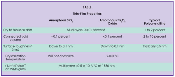
For the amorphous films used in telecom
filters, the effects of water absorption are essentially nonexistent because of
their low void volume (see table). The filters remain within the wavelength specification
of ±0.1 in 1550 nm (0.0065 percent) from dry to moist air conditions —
i.e., one-eighth of the wavelength separation between adjacent channels on the 100-GHz
ITU grid. Errors outside this range introduce crosstalk.
Absorption losses in Ta2O5 due to incomplete
oxidation also lead to transmission losses, but very thorough oxidation of the Ta2O5
is achieved by oxygen-ion bombardment of the growing films in both the ion-beam-sputtering
and plasma ion-assisted electron-beam processes. Transmission losses in a 100-GHz
filter result from even a small amount of absorption from substoichiometric Ta2O5
(Figure 1). However, for fully oxidized material, Ta2O5 exhibits one of the lowest
absorption coefficients for high-index oxides and is therefore a good choice for
filters.
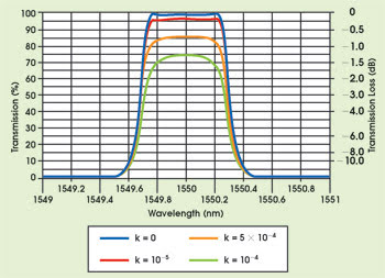
Figure 1. The spectra of 100-GHz filters
display increasing transmission losses as the extinction coefficient (k) of Ta2O5
increases. Fully oxidized amorphous Ta2O5 films, as well as good quality SiO2 films,
have extinction coefficients in the range of 10—6. DWDM specifications permit no
more than 0.5 dB of insertion loss for filters (greater than 89 percent transmission).
To ensure stability over decades of
service, the amorphous materials should not begin to transform to the more thermodynamically
stable crystalline state. Here, too, Ta2O5 is the best high-index material. Compared
with other candidates, such as TiO2, HfO2, ZrO2 and Nb2O5, amorphous Ta2O5 has the
highest crystallization temperature (more than 400 °C). SiO2 will remain glassy
even at much higher temperatures.
Compensating for temperature
Precise quantification of the characteristics
of the amorphous materials has been made possible because the multicavity etalon
filters have extremely sharp transmission peaks and because of the availability
of the very precise telecom lasers used to measure shift. These new capabilities
in test and measurement have promoted solutions to the thermal problems facing telecom
components. DWDM filters must display extreme wavelength stability over an operating
range of 0 to 65 °C. This cannot be achieved based on the material properties
of the amorphous coatings alone.
Counterintuitively, the answer is to
use a glass for the substrate that displays a higher coefficient of thermal
expansion than the coating. As the temperature rises, the glass expands and stretches
the coating, thereby reducing the coating’s thickness. Glasses such as WMS
have been developed so that this thickness reduction compensates almost exactly
for the average change in the optical thickness — i.e., the refractive index
multiplied by the thickness — with temperature (see table).
Commercial glasses formulated to meet
this need feature coefficients of thermal expansion of 10 x 10—6/°C to 11 x
10—6/°C. The typical temperature shift of filters constructed on such substrates
is less than 1 pm/°C at the center wavelengths, which corresponds to a shift
of less than 0.065 nm over the operating temperature range.
Such measurements have established
the thermal stability of the films far more precisely than previously possible.
Even for the common substrate glass BK 7, which displays a coefficient of thermal
expansion of 7.1 x 10—6/°C, measurements have revealed excellent thermal stabilities
that would exceed the requirements for precision optics in applications outside
of telecommunications.
New monitoring approach
The production of DWDM filters also has necessitated
a new approach to optical monitoring. Rather than sampling a succession of test
glasses, telecom component manufacturers have had to test the parts themselves to
avoid tooling factor issues. Improvements in optical monitoring and the use of
stabilized telecom lasers have enabled manufacturers to accurately monitor even
low signal intensities, and automated predictive algorithms have been developed
to ensure an accurate endpoint cut on the turning points of the λ/4 layers.
For example, the variation in transmission
intensity during deposition for part of a 100-GHz filter declines to a few percent
of the initial value through the layers of the first reflector stack (Figure 2).
Automatic gain changes maintain a high precision even at these low levels, enabling
precise monitoring of the 10 λ/4 spacer layers before the transmission again
increases as the next reflector stack is deposited. This cycle is repeated for the
remaining three cavities.
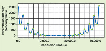
Figure 2. Improvements in optical monitoring enable manufacturers to accurately monitor the deposition process even at low signal intensities. Here the transmission signal
during the deposition of a 100-GHz filter (showing only the first of four cavities)
declines to a few percent of the initial value through the layers of the first reflector
stack.
But still another feature is required
to obtain the accuracies necessary for telecom applications. Inaccuracies tend to
be compensated in successive layers when cutting on λ/4 swings.4 This occurs only
when the cumulative transmission or reflection is measured, and not when individual
test glasses are used, as in general optics. Run-to-run wavelength reproducibilities
of better than 0.1 in 1550 nm (0.0065 percent) can be achieved for DWDM filters
because of optical error compensation, despite the fact that the errors on individual
layers are larger than this.
Lastly, to increase the yield from
the monitored regions, manufacturers have turned to employing discs of glass up
to 12 in. in diameter. These discs are typically 7 to 10 mm thick and are thinned
down and diced after coating to produce the small filters. Much attention has been
given to wobble-free mounting, and wobble of less than 0.02° has been achieved
while rotating the disc at speeds of 500 to 1000 rpm, which evens out the deposition.
Process development, automation
Process endurance and stability have been extended
significantly to complete the 100- to 200-layer filters, which are 25 to 50 μm
thick. For ion-beam sputtering, special attention has been given to the design and
operation of the beam extraction grids. For plasma ion-assisted electron-beam evaporation,
special high-capacity hearths have been developed. The oxygen-ion conditions for
both processes have been optimized to produce fully oxidized films, while maximizing
the deposition rate and minimizing the stress.
Although the stresses in amorphous
films are generally higher than in polycrystalline films, they are acceptable for
optics with an aspect (diameter to thickness) ratio of up to two — such as
the small filters obtained after dicing — and for a wide range of general
optics. Despite their thickness, DWDM films pass the Scotch tape test, are very
hard and robust, and survive the dicing process with minimal chipping. For thinner,
general coating designs, the effects of stress are lower, and the aspect ratios
can be larger. For thin antireflection coatings, stress effects are negligible.
Much effort also has been put into
uniformity. Quartz crystal monitors may control the electron-beam profile. Masks
or a fine control of the substrate and of the target angles may control the ion-beam
flux. These are welcome developments for general optics, in which larger uniform
areas are sought.
With deposition times ranging from
10 to 50 hours, reliable operation is essential, and intelligent automation is supplying
this capability. Process parameters are monitored for conformance and are regularly
logged, and the systems are designed to shut down safely in the event of any malfunction.
Unattended operation is common.
Optical programs calculate the approximate
turning-point transmissions so that the gain setting for each layer may be determined,
and the type of fitting for the reflector, spacer and coupling layers in the structure
is programmed. Unlike the traditional, operator-determined cut point, there is no
need for operator intervention.
Automated coating machines, employing
either ion-beam-sputtering or plasma ion-assisted electron-beam technologies, are
producing amorphous materials for precision optics. These machines will revolutionize
the manufacture of high-precision optics, ranging from more precise edge or pass
filters, wavelength-selective coatings, and precise, broadband antireflection coatings
to other coatings that are at the limits of traditional technology.
Hundreds of coating machines have already
been installed with the special features required to produce amorphous films. The
widespread acceptance of the qualities of amorphous films is bound to stimulate
interest in coating applications that are not achievable with conventional processes.
For example, the range of materials
that can be deposited in amorphous form is bound to increase. The common coating
materials Al2O3, Ta2O5, TiO2 and SiO2 are produced naturally in the ion-beam-sputtering
process. Here the energy of the depositing atoms is in the range of 1 to 10 eV,
providing enough mixing energy to prevent crystallization. These materials traditionally
have been used where the lowest losses, down to a few parts per million, are required,
such as in laser gyro mirrors.
In plasma ion-assisted electron-beam
deposition, the mixing energy to prevent crystallization comes from the plasma potential.
This can cover a range of process conditions and enables the production of films
from polycrystalline to amorphous, including dense amorphous TiO2, Ta2O5 and SiO2.
The durability of amorphous multilayer
coatings and the ability of automated machines to deposit them also enable the fabrication
of more complex designs featuring hundreds of layers. Many desirable coating features
can be enhanced by designs with more layers. For example, pass/block bands may be
made closer together to separate closely spaced wavelengths, or the tolerance of
various angles of incidence and polarization properties may be increased. Moreover,
wider reflective, output coupler and antireflective bands can be achieved.
Monitoring thick layers
The means exist to deposit coatings up to 50 μm
thick (approximately 200 layers at 1550 nm, or approximately 600 layers in the visible).
This is beyond the scope of either quartz crystal or optical test glass monitoring.
For the multicavity etalons for telecom, however, laser-based transmission or reflection
monitoring has proved an excellent solution. To employ these techniques for etalons
at different wavelengths requires only the use of lasers with the appropriate wavelengths.
Advanced computer algorithms will help extend optical monitoring to other coating
designs.
For applications that do not require
the extreme precision of DWDM filters, however, time-based monitoring may be appropriate.
It is not limited by thickness or wavelength, and requires neither crystal nor test
glass monitors, nor an optical pathway in and out of the deposition chamber. Rather,
its precision is dependent on the ability to maintain predictable process conditions
between calibration and parts runs.
The reproducible process conditions
of load-locked ion-beam sputtering machines, which are used throughout the semiconductor,
magnetic head and diode laser industries, make them suitable for use with time-based
monitoring for the production of coatings with very many layers. The sputtering
process typically uses large plates or discs as the source material, which last
for numerous runs, so there is no reason to open the door of the main process chamber.
Because the sputtering process is reproducible, these processes usually are controlled
by time, eliminating the expense and inconvenience of replacing quartz monitor crystals
or optical monitor chips — because neither is required. This concept has been
extended to the larger chambers used for optical ion-beam sputtering (Figure 3),
enabling the high-volume manufacture of precision optics and opening the way for
complex designs with possibly hundreds of layers.
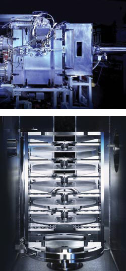
Figure 3. The reproducible process conditions of ion-beam sputtering with a load lock make it suitable for use with time-based monitoring. For the shorter runs that are typical
in the manufacture of general optics, the throughput of the load lock compensates
for the slower deposition rate ascompared with electron-beam deposition. The 12-in.-diameter
optics inside the load lock are shown below. Courtesy of Nordiko.
The enormous strides made in the production
of filters for telecommunications offer the opportunity to upgrade traditional coating
techniques, thus reducing production uncertainty and atmospheric drift to enable
greater precision. Moreover, automation and the robustness of the amorphous materials
will facilitate the production of more complex coatings, opening up new applications
for coatings beyond telecom.
References
1. A.T. Howe and D.D. Phillips (1995). Use of
ion beam sputtering in the fabrication of high quality optical coatings for laser
and telecommunication applications. Proc. SPIE.
2. A. Zoller et al (1996). Temperature-stable
bandpass filters deposited with plasma ion-assisted deposition. APPLIED OPTICS,
Vol. 35, pp. 5609-5612.
3. C. Langhorn and A. Howe (June 1998).
Optical morphology: Just how smooth is that surface? PHOTONICS SPECTRA, pp.
130-133.
4. H.A. Macleod and D. Richmond (1974).
The effect of errors in optical monitoring of narrow-band all-dielectric thin film
optical filters. OPTICA ACTA, Vol. 21, pp. 429-443.
Meet the authors
Arthur T. Howe is president of Chromatel, a consulting
company in Auburn, Calif.
Mervyn Davis and David Pearson are
technical director and process development manager, respectively, at Nordiko Ltd.
in Hampshire, UK.