As the semiconductor industry explores next-generation lithography, the old generation still has a few tricks up its sleeve.
Hank Hogan, Contributing Editor
The $140 billion-a-year semiconductor industry depends on Moore’s law, the decades-old
observation that device density doubles every 18 months or so. Today, excimer lasers
power optical photolithographic tools that help drive this march toward smaller
features. These tools routinely print millions of polymer resist lines that are
hundreds of microns long and less than 0.2 μm wide.
The conventional wisdom in the industry indicates
that fundamental changes loom in photolithography. The most common steppers use
lasers operating at 248 nm. By the end of the decade, state-of-the-art tools are
expected to use 13.4-nm sources. Dubbed extreme-ultraviolet (EUV) technology, this
projection print approach applies UV radiation, but unlike its predecessors, it
must operate in a vacuum and requires reflective, not refractive, components.
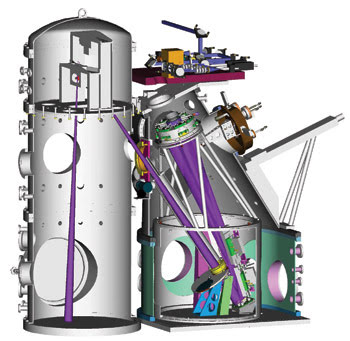
The semiconductor industry must reinvent everything to perform EUV lithography, from the light source
to the optics to the photoresist. Although the industry is well on its way to developing
EUV technology, the remaining challenges have engendered discussions about how far
optical techniques can be extended. Courtesy of Sandia National Laboratories.
“EUV is more of a revolution
from optical lithography as we know it today,” noted Tony Yen, director of
lithography at International Sematech in Austin, Texas. Sematech is shooting for
the first EUV application in 2007, but Yen said that it may not occur until 2008
or 2009.
Not everyone agrees that EUV, which
some claim is closer to x-ray than to optical technology, will be deployed by then
or that it is even necessary. Optical lithography advocates point to published research
describing the printing of lines narrower than the wavelength of the source. This
occurs to some extent every day in microchip manufacturing, but research suggests
that the limits of subwavelength lithography could be extended. At Massachusetts
Institute of Technology’s Lincoln Laboratories in Lexington, staff member
Mike Fritze printed a 9-nm-wide line using a 248-nm source. By contrast, today’s
most advanced commercial products have minimum feature sizes of 70 nm or more.
Phase-shift technology typically enables lithographic processes to
produce features with dimensions measuring half the source wavelength, but research
suggests that the technology can enable features 1/10 of the source wavelength. The gate sizes shown are, from left to right, 90, 25 and 9 nm. All were produced using a 248-nm light source. Courtesy of Lincoln Laboratory.
First reported in 2001, Fritze’s
results were for an isolated line and for experimental purposes, but they indicate
what might be accomplished with the application of resolution-enhancement technology.
“In my own opinion, for this decade, we’re likely to use optics and
extensions,” said Fritze, who researches resolution-enhancement technology
as part of Lincoln Laboratories’ Advanced Silicon Technology Group.
On the other side of the continent,
Eli Yablonovitch, an electrical engineering professor at the University of California,
Los Angeles, had a bolder response when asked how long optical techniques can continue
to power semiconductor manufacturing: “The simple answer is there is no limit.
What people previously believed was the limit, which is the Rayleigh criterion,
was misinterpreted. The Rayleigh criterion is a limit on density, not a limit on
linewidth.”
The Rayleigh limit, he said, applies
to pitch, which is line density or linewidth and spacing. The limit is half the
wavelength of the light source, divided by the numerical aperture of the optics.
Challenging reflections
The semiconductor industry has determined that
the best way to surmount the pitch constraint is to cut the wavelength of the source.
Tools based on 193-nm ArF sources are replacing those based on 248-nm KrF lasers.
By the end of 2005, according to Yen, F2 lasers at 157 nm will define state-of-the-art
manufacturing. Lithography tools based on these sources all use transmissive optics,
firing the beam through a photomask and various lenses to image circuit elements
onto a target wafer.
At 13.4 nm, however, EUV tools represent
more than a tenfold reduction in wavelength over their immediate predecessor. That
will drive pitch down correspondingly. The problem is that transmissive optics are
no longer an option at EUV wavelengths.
“You have to switch from refractive
optics to reflective optics,” said Bob Sell, manager for marketing and strategy
development for semiconductor materials at Corning Inc. in Corning, N.Y., which
supplies optical blanks to the semiconductor industry for use in photolithographic
tools. “No material is going to transmit the 13.4 [nm radiation]. In fact,
it has to be done in a vacuum because it won’t even go through air.”

Despite the challenges
that calcium fluoride presents to 157-nm lithography, it is still a transmissive
and, therefore, familiar technology to semiconductor manufacturing. The next step
after 157-nm processes could be EUV lithography, which requires all-reflective optical
components. Courtesy of Corning Inc.
The change from refraction to reflection
has a number of implications. For one thing, refractive transmission can be higher
than 99 percent. Thus, nearly all of the fluence ends up at the target. Such is
not the case for reflective processes, particularly at 13.4 nm, in which the radiation
reaching the target drops to about 70 percent. That reduction affects throughput
of the tool, the lifetime of the optics and the rate at which the source is consumed.
Sell said that Corning plans to offer
the semiconductor market an ultralow expansion material called ULE, currently used
in the reflective optics of large telescopes. ULE has not found use in microelectronics
manufacturing before, but Sell is confident that it can work.
However, not everyone believes that
reflective optics operating in a vacuum with a 13.4-nm source is the wave of the
future. Some argue that Fritze’s work offers a potential alternative, if aided
by resolution-enhancement techniques such as optical proximity correction.
This approach anticipates printed distortion
in corners or at the end of bars. The layout of the circuit on the mask is altered
in such a way as to remove some of that distortion and to allow the pattern to print
much closer to its intended shape and size.
Because a photoresist captures radiation,
it also captures interference patterns. That can be exploited, Fritze said, to produce
a dark line whose width is half that of the exposing wavelength. This is done today
on critical layers that have the smallest feature sizes and that typically define
the electrical width of the transistors.
With feature slimming, researchers
can make resist lines even smaller by uniformly etching them away. These and other
techniques enable an isolated line to be narrowed down to virtually nothing —
or until it becomes mechanically unstable.
“That’s very useful, of
course, for doing research when you don’t have to pack things very densely,”
Fritze said.
Although he has achieved this in a
research lab, such subwavelength tricks are also finding a home in large-scale manufacturing
of the latest microprocessors, in which features are crammed close together. As
in Fritze’s work, these techniques use interference-producing phase-shifted
masks, designed with software tools and technology from Numerical Technologies Inc.
of San Jose, Calif.
However, although isolated lines can
be made arbitrarily small, lines embedded within a dense thicket of neighbors cannot.
One solution is to apply phase-shift techniques in a double exposure to pattern
one layer of the resist. In this method, half the features are on one mask, and
the other mask holds the rest. Dense structures would be interdigitated. This divide-and-conquer
approach pays dividends in terms of minimum achievable pitch.
“A double exposure is equivalent to cutting the wavelength in half,” Yablonovitch said.
This could be carried even further
with three or more exposures. With a higher numerical aperture and double exposure,
the achievable density would more than double. The problem of registering one half
of the layer to the other would be no worse, Yablonovitch noted, than aligning
separate layers to each other. In an advanced semiconductor process, both would
be equally challenging.
Multiple exposures present potential
problems for the photoresist, said Mark Slezak, a technical manager for JSR Micro
in Sunnyvale, Calif. The difficulty arises because the features are split among
two or more masks. Often, one mask will image critical but isolated structures,
and the other will image larger features with tighter pitches. During processing,
both masks go through the same tool and are exposed to the same source to produce
the final image in the resist. Thus, the resist can register not only imaging differences
between the two masks, but also any subsequent development and processing differences
related to the dissimilar feature sets.
“This makes the resist vulnerable
to bias issues that can be enhanced by not only the aerial image of the exposure
tool, but also the acid diffusion properties inherent to the material,” Slezak
said. “A well-balanced photoresist is important in these situations.”
Another concern arises from resist-slimming
techniques, which often are chemical in nature. This is independent of the source,
but the interaction of the fluence and the chemistry can be complicated and must
be addressed.
Hence, phase-shifting and optical proximity
adjustments require interaction with and information from the manufacturing process,
said J. Tracy Weed, a senior director of marketing and business development for
Numerical Technologies.
“There’s a very intricate
feed-forward/feedback loop that has to be maintained in order to create manufacturable
features,” he said.
Weed thinks optical processing will
continue to be the semiconductor workhorse for the foreseeable future. He noted
that the lifetime of optical lithography will be extended by chemical mechanical
polishing techniques, which use a slurry of small particles to grind wafer surfaces
flat and allow imaging with smaller depths of focus.
Chemical mechanical polishing techniques
are important to the discussion of overcoming pitch limitations. Numerical aperture
is part of the formula that specifies minimum pitch. In standard photolithographic
tools, air or an inert gas occupies the optical path, and filling that path with
the right fluid can boost numerical aperture and cut the minimum pitch. Optical
microscopists have used this approach successfully for years.
However, increasing numerical aperture
decreases the depth of focus. Hence, planarization becomes more important and innovations
such as chemical mechanical polishing more vital.
Applying fluid to the optical path
raises other concerns for tool manufacturers. “You might have currents and
eddies, and you’ll have to deal with those types of distortions, but it sure
beats making a multilayer reflective mask that has to be accurate to atoms in terms
of planarity and uniformity,” Weed said.
The question of when optical techniques
will no longer represent the cutting edge of lithography is one of economics. Both
sides’ arguments boil down to the cost of multiple exposures vs. the cost
of new light sources and infrastructure.
Multiple exposures mean that the number
of masks increases. This may be done only on critical layers, but it still has an
impact. For phase-shift masks, the number of critical mask layers will increase
fourfold or more. Each mask requires separate exposures, requiring separate trips
through the tool. That cuts into the tool’s effective throughput and makes
it less economical to operate.
Final analysis
“First, you have to have a number of these
masks, and masks are very expensive,” said Sematech’s Yen. “You
get expensive masks, and you lose the throughput. So you are being hit twice. That
may not be a practical approach.”
Conversely, radical changes in the
source and the infrastructure also are expensive. New optical components have to
be developed and new resists perfected. Also to be considered are the cost of the
source itself and the possibility of process changes necessitated by the new resist.
“Now, do you think that something
that has half the wavelength is only going to cost twice as much? It’s going
to cost a lot more than twice as much,” Yablonovitch said.
It’s too early for the industry
to make a final decision. However, the latest microprocessors are emerging from
248-nm photolithographic tools, suggesting that these sources are producing commercial
devices with features at least 95 nm in size. That partly is because more advanced
tools are either not available or too costly, which suggests that EUV may take longer
to arrive and be deployed than current plans demand.
“The development costs are going
up,” said Corning’s Sell. “I think [that] people work very hard
to stretch the existing technology. So we’re already seeing 248 [nm] being
used today for a node that, five or six years ago, no one thought 248 [nm] would
be used for.”
Other contenders
While EUV lithography
is the designated heir to current semiconductor manufacturing methods, others could
also be contenders. Some of these may even be successors to EUV.
Direct-write electron-beam technology, for instance,
offers small linewidths and tight pitches. It currently is used to create the photomasks
employed in today’s optical techniques. However, it writes each wafer and
every line individually, in contrast with optical methods, wherein photons flood
the surface and transfer the layer information all at once from the mask to the
wafer.
“No serial processes can be faster
than that,” said Tony Yen, director of lithography at International Sematech
in Austin, Texas. “You — boom — hit it and then you get the pattern.”
Another possibility is the use of x-rays.
In this approach, a mask is brought close to the surface of a silicon wafer coated
with resist. The mask is exposed, and the pattern transferred to the resist. This
process suffers from a number of problems, including the need to research and develop
resists, masks and x-ray sources.
At the University of Texas in Austin,
Grant Wilson’s research team is working on another technique, step-and-flash,
which applies a quartz mask carrying high-resolution relief images directly to the
surface of a resist-coated wafer. After photopolymerization of the resist through
the back of the quartz template, the mask is removed, leaving a UV-cured replica
of the relief structure on the planarization layer. Step-and-flash techniques have
reliably produced features smaller than 60 nm.
However, this and other nano-imprinting
methods require the construction of a mold, which sounds no more difficult than
making an optical photomask. But optics reduce a photomask’s pattern to the
right size on the wafer, allowing mask makers to reliably and inexpensively produce
high-quality products. That approach isn’t possible when using a mold, Yen
noted.
“If you want to write the features
on a mask the same size as the features on a wafer, [then] that mask is really tough
to make,” he said.
For these and other reasons, Sematech
and its member companies have decided that EUV represents the best choice for what
has been called next-generation lithography — for now.