Herbert Pummer, Exitech Inc.
Fully integrated laser-based micromachining systems are gaining acceptance in several areas of display manufacturing. These include processing of a broad range of materials that compose the display itself and large-area micropatterning of polymers to facilitate light management in transflective displays.
One application involves the transparent conductive oxide electrode layer (ITO is a common material). A large plasma display panel, for instance, will contain several million pixels. Using high-power multimode Nd:YAG lasers at 1.06 μm, Exitech micromachining systems can pixelate a 42-in. panel in less than a minute.
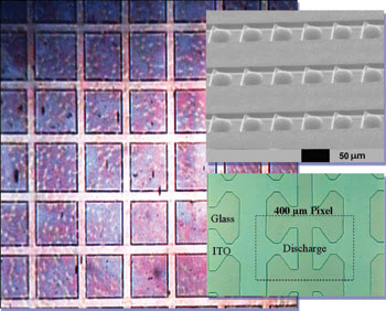
Examples of laser micromachining in display applications include microlenses on 45° ramps (a),processing of 50-μm bands in Orgacon El-350 material on 175-μm PET (b) and pixelation of ITO for plasma display panels (c).
To handle this application, engineers use a technique called bow-tie scanning. This one-step, high-yield dry process compares favorably with the conventional multistep lithography/wet processing approach that requires more expensive machines and that introduces waste-removal issues. The laser process is especially cost-competitive when manufacturing 42- to 61-in. panels.
Laser patterning is also of interest when manufacturing a large number of different screen designs, each type in low to medium volumes — specifically when using direct-write processes for manufacturing specialty screens or rapid prototyping. Switching among many designs usually requires no more than entering different CAD files. It is also possible to pattern transparent conductive oxide on glass and on flexible substrates that can be produced reel to reel.
Other materials micromachined in display applications include light-emitting polymers and those used for barrier layers. Engineers must remove these materials to allow device frame preparation prior to encapsulation and generation of vias. For some of these materials, laser processing is essential at present because they must be processed in a vacuum or in an inert gas environment. This is why the firm’s M5000P laser system for high-speed processing of large panels also has the option to process in a glove box.
Other applications include high-speed and precision patterning of thin metal layers, such as the cathode in polymer and organic LEDs. These usually use excimer lasers and mask projection techniques.
Laser systems also can handle direct-write exposure of thick-film photo-printable layers and dry-film resists. Using 355 nm, these systems can expose a total line length of 1 km in one minute. Applications include exposure for bus and address electrodes and barrier rib formation in plasma display panels.
The second area of strong interest in display manufacturing is light management in transflective displays. The display can represent more than half of a device’s power consumption, and, at present, no more than 10 percent of the backlight’s output may be directed toward the viewer. This has substantial impact on battery size and lifetime for nomadic devices.
Seeing the light
One way to increase lighting efficiencies for displays is to direct more backlight through the pixels. These applications use arrays of micro-imaging elements, including spheric and aspheric lenslets, strips of cylindrical microlenses and pyramidal and other shapes. Such individual micro-optical elements may range in size from several hundred microns to less than 10 μm, and they are needed in sheets that match the size of the display. Manufacturing them can be a challenge. Even when the structures lend themselves to diamond machining, the process tends to be time-consuming, and turnaround times, often of months, can be obstacles to rapid prototyping and the manufacture of masters for production.
To address some of these issues, Exitech recently developed the PPM-1600 laser machining system for large-area micropatterning of polymers. In the process, the desired mathematically defined surface topology is translated into a multiaperture photomask. Using a method called synchronized image scanning, the photomask laser etches the desired topology onto the polymer. This can then be used directly or to generate a master for replication.
The laser-based micromachining system has substantial flexibility with respect to the structures it can produce, and it typically can write areas of 4 × 4 in. in less than 30 minutes. Sheets with a total area of up to 1.4 × 1.4 m can be patterned.
Contact: Herbert Pummer, president, Exitech Inc., Foster City, Calif.; +1 (650) 212-1411; +1 (650) 212-1511; e-mail: [email protected].