The key to successful diode manufacturing lies in the careful choreography of all critical build stages, from epitaxial growth to packaging.
Paula M. Powell, Senior Editor
By one estimate, the global market for high-power laser diodes could approach $450 million by 2006 (Figure 1). So it perhaps comes as no surprise that quite a few players have entered the market recently. To compete, they must accommodate increasingly sophisticated end users who are demanding higher output power, higher brightness and longer device lifetimes.
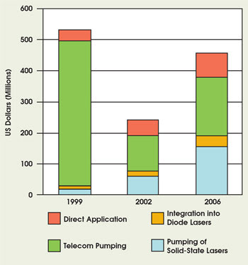
Figure 1. According to Arnold Mayer at Optech Consulting, market projections include the value added by packaging the diodes, but not the value added by stacking or fiber coupling.
The key to standing out in this field lies in providing these capabilities at a competitive price. This requires a sound understanding of the manufacturing process, from epitaxial wafer growth to packaging.
Consider diode lasers for pumping solid-state lasers and direct applications. According to Maørc Kelemen, a researcher with the Fraunhofer Institute for Applied Solid State Physics in Freiburg, Germany, diode lasers increasingly require a combination of high beam quality and output power. To compete in industrial applications, though, companies also must contain device fabrication costs.
In one example, researchers at Fraunhofer resolved these seemingly conflicting requirements using a tapered diode with a ridge waveguide. This device, which recently was commercialized by Freiburg-based M2k-laser GmbH, has a single-quantum-well InGaAs/AlGaAs structure and emits wavelengths between 0.8 and 1.1 μm. Kelemen said that, with this design, the length of the tapered structure basically determines the output power, while the brightness is dependent on the length of the ridge-waveguide structure. The researchers are working on extending the emission capabilities to 2 μm for other applications.
When things heat up
Companies also need to understand the inherent heating characteristics of semiconductor lasers. Stan Whiteley, a research scientist with Cutting Edge Optronics Inc. in St. Charles, Mo., said that the continued emphasis on higher power, higher brightness and longer life presents some basic problems for companies manufacturing high-power diode bars. “Devices typically generate at least 10 times the heat flux of any other semiconductor device,” he said, “which can translate to a need to remove kilowatts of heat from a big array. As efficiency improves, the devices generate a little less heat but then produce more power, which puts some heat back into the system, making it difficult to reduce heating of semiconductor lasers beyond a certain point.”
In addition, optical power density at each diode facet can reach megawatts per square centimeter. Whiteley reported that, for this reason, engineers must be extremely sensitive to any optical absorption, reflection and loss. Facet coating becomes an extremely critical step in the fabrication process (Figure 2).
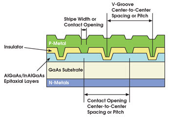
Figure 2. A common high-power laser diode bar produced in the foundry of Cutting Edge Optronics can have up to nine layers.
To top that, such devices operate at very high optical currents, with upward of 100 A flowing into an extremely small bar. Current densities can reach 200 A/cm2, which is greater than the density typically allowed in copper wires.
Producing light without melting something often depends on the packaging of the diode, including the heat sink. Guido Bonati, manager of product development at Jenoptik Laserdiode GmbH (JOLD) in Jena, Germany, believes that the answer to boosting output power and life could lie in rethinking the cooling strategy. Over the past several years, Bonati and his colleagues have promoted a passive cooling strategy to replace microchannel heat sinks. Their research has shown that, in many cases, the semiconductor materials are no longer the factor that is limiting the lifetime of high-power laser diodes. The heat sink is.
According to the scientists, a typical microchannel heat sink delivers cooling fluid through different copper layers that act like a manifold. Diode lasers producing output in the 50-W range currently require the use of microchannel heat sinks. Conventional passive options are limited to the cooling of diodes with a maximum output of 40 W; however, there are several potential problems related to the use of microchannel heat sinks. One, Bonati noted, is that diode lasers rated at 50 W have limited lifetime (approximately 15,000 to 20,000 hours), in part because erosion and corrosion affect the efficiency of the cooling system.
JOLD engineers have been working for some time to deliver a passive solution that works with higher-power laser diodes. One issue they resolved was the size of conventional passive heat sinks, which limited the pitch of laser diodes (distance between the centers of each bar) when building up a horizontal stack for pumping rows (Figure 3).
Figure 3. A virtual passive cooling strategy developed by Jenoptik reportedly allows extension of the benefits of passive cooling to high-power laser diodes with output of 50 W. Tests indicate that laser diodes using the company’s new heat exchanger/heat sink concept have lifetimes as high as 30,000 to 50,000 hours, depending on the semiconductor materials used.
Layered design
Their enhanced virtual passive cooling strategy, which was introduced at Photonics West in San Jose, Calif., last month, reportedly can support an increase in power to 50 W per bar, while allowing lifetimes in the range of 30,000 to 50,000 hours for selected laser diode materials. The concept involves layering a passive heat sink on top of a patent-pending heat exchanger designed specifically for passive heating.
This design has several copper layers, much like a microchannel heat sink, but has an inner structure designed to ensure that erosion is no longer an issue. Some of the copper layers are coated with additional ceramic materials that are then plated with a copper layer to build up the electrical connectors. The goal, according to Bonati, is to separate the water circuit from the electrical potential and to eliminate any electrogalvanic effects. Another benefit is that it eliminates the need for deionized water.
Even with increased lifetime, though, end users are still faced with the fact that the failure of laser diodes cannot be predicted. So that this limitation would not hinder the benefits of high power and long life, the German researchers devised a bypass circuit to account for random failure of a diode in the pumping row.
Perhaps an even more ambitious project is that of the Super High Efficiency Diode Sources program sponsored by the Defense Advanced Research Projects Agency in Arlington, Va. One of its primary goals is to boost electrical-to-optical efficiency of stacks of diode laser bars to 80 percent within three years.
Martin Stickley, program manager for the agency’s Microsystems Technology Office, said that the target parameters are efficiency, spectral definition and power output. The investigators are shooting for 65 percent efficiency from a laser bar, a spectral width of 2 nm with a spread of no more than ±0.5 nm over the length of the bar and 80 W of output power within 18 months. The goal for 36 months is 80 percent efficiency of a stack of bars, with the same spectral width and spread of the emitting regions and 480 W of output power. A 480-W stack would thus use six 80-W bars.
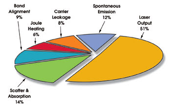
Figure 4. In this example illustrating areas of power consumption in a typical 980-nm bar, electrical-to-optical efficiency is 51 percent for a bar that produces 40 W of optical power. Therefore, 78 W of electrical power would be the input. As part of a Defense Advanced Research Projects Agency project to boost efficiency of high-power diode lasers, Alfalight is working to reduce power consumption in each of these areas.
Manoj Kanskar, vice president of research and development for Alfalight Inc. in Madison, Wis., believes that the 18-month goal is achievable with incremental improvements in current technology (Figure 4). The company’s 980-nm device, based on GaInAsP, is already at 55 percent efficiency. He agrees with Stickley, however, that evolutionary improvements in diode fabrication alone probably will not be enough to reach the final project goal.
What needs to be done
Stickley said researchers must work on areas that go beyond straightforward improvements, including:
• Development of transverse junction stripe designs to bypass heterojunction barriers and achieve superefficient injection.
• Use of photonic bandgap structures to reduce spontaneous emission into undesired modes and thus improve the gain and lower the threshold.
• Use of quantum dots to reduce the threshold.
• Crystal growth on GaAs with a different crystalline orientation to increase the gain.
Conventional areas to be addressed include developing asymmetric waveguides to reduce optical absorption, interface bandgap engineering to reduce heterojunction voltages, reduction of series resistance and improvement of carrier confinement.
According to Kanskar, an increase in diode efficiency will dramatically reduce the waste heat that must be removed from a high-power diode-pumped solid-state laser system. With diode-laser pumping at 980 nm, slab lasers typically have optical-to-optical efficiency of 50 percent. An application that calls for 25 kW of output requires 50 kW of pump power from the diodes, which today would require 100 kW of electrical input. Altogether, 75 kW of waste heat must be removed from the system. If one boosts the efficiency out of the diode stack to 75 percent, waste energy is reduced almost by half, to 42 kW. Kanskar noted that a relatively small gain in efficiency of stack output saves twice, once in the electrical power supply and once in reduced waste heat.
The thirst for increased output power extends even to the newest types of laser diodes, which present some interesting challenges to end users who are used to working with more durable laser diode types. For instance, one must come up with a strategy to package the new generation of blue, violet and UV diodes and protect them against mechanical shock and electrostatic discharge without limiting the features that make them useful in sensitive biosensor applications. Dan Callen, product manager at Coherent Inc. in Auburn, Calif., said that, at least for the present, the systems integrator must find a way to improve device durability to protect it against mechanical shock and electrostatic discharge. And considering that the cost per device can reach $3000, few companies in this category can afford a long learning curve in their efforts.
“While there may be some patent issues hindering efforts to package the device for this level of protection in its raw state,” he said, “we are hearing rumblings from the foundry guys about resolving these issues. Until solutions reach the market, though, end users are faced with a laser diode that is fairly delicate in the state it arrives from the manufacturer. The diodes can easily pick up electrostatic discharge and turn it into unwanted laser light.”
Coherent, which also manufactures diodes at other wavelengths, serves as a systems integrator in packaging violet laser diodes for biophotonics and other applications. Engineers protect these solid-state UV diode laser systems based on InGaN technology by surrounding them with several layers of metal electrically shielded and directed to an earth ground. To further improve lifetime, modules such as the company’s Radius 375-8 also have a built-in fan system to facilitate cooling and reduce end-user concerns about heat dissipation. This product is designed for applications such as biological and chemical detection, confocal microscopy, flow cytometry and semiconductor test and measurement.
Ultimately, regardless of the laser type, diode designers appear to have several priorities of varying importance. The first seems to be enhancing power, followed by lifetime, with these requirements varying based on the application. Durability, such as is discussed by Callen, is perhaps fourth, after capability for high-temperature operation.
Telecom Rethinks Manufacturing
Within the telecom and datacom markets for laser diode technology, vendors are increasingly cost-conscious —but they also are gaining manufacturing savvy in parallel. Consider, for example, the idea of streamlining the manufacturing process to cut costs. Dublin, Ireland-based laser diode manufacturer Eblana Photonics, which has a range of 1550-, 1490- and 1310-nm devices for broadband communications, reports that it uses a proprietary process to eliminate a regrowth step that not only gives it better process control, but that also facilitates outsourcing of epitaxial growth.
Another interesting effort along this line involves the building of laser diodes with facets that are etched rather than mechanically cleaved into the semiconductor wafer. According to Alan Morrow, vice president of technology development at BinOptics in Ithaca, N.Y., the company recently introduced 1310- and 1550-nm lasers for datacom and metropolitan applications that are based on a patented etched-facet technology developed at Cornell University.
“In most processes used to make laser diodes, the wafer must first be scribed and cleaved to separate the diodes and create the output facet to let the light exit,” he said. “The problem with this approach is that you don’t actually create the device until you’ve broken the wafer, so you can’t tell how it will perform. In addition, traditional process steps like cleaving can have very low yields.”
In the etched-facet process, a photolithographically defined layer of material is deposited on the top surface of the semiconductor, allowing vertical facets to be precisely etched without cutting up the wafer. The company reports that, as a result, it can test the devices in wafer form when they are easy to handle and locate. The technique also allows monolithic integration of additional functions on the same chip. For example, BinOptics can integrate a monitoring photodetector with its lasers, saving space and assembly costs.
This technique also can eliminate process steps, potentially cutting costs. Morrow uses the example of a 10-Gb laser requiring a distributed feedback grating. After the laser structure is made, the grating is etched on the surface very close to the active region to control its operating wavelength. It is then necessary to grow a layer of crystalline semiconductor material on top of the grating to get good diode reliability. The process can achieve similar results through the use of etched etalons. These structures comprise mirrors spaced very close together that perform the same function as the grating but that are reportedly far less costly to fabricate because no regrowth is required.
Working to simplify the laser diode process on two fronts — manufacturing and integration of devices into the network — is CyOptics, which has wafer and chip fabrication facilities in Yokneam, Israel, and automated packaging and testing in Lehigh Valley, Pa. Last year, the company introduced a 2.5-Gb/s uncooled 1.55-μm distributed feedback laser with an operating temperature range from –20 to 95 °C. According to Robert Hartman, vice president of device design and development, this laser expands uncooled systems into new application areas and decreases costs by eliminating the need for cooling.
The company, a developer of InP devices for fiber optic communications, has just been awarded a patent for a two-lens arrangement used to couple light from its lasers into an optical fiber in a laser package. This reportedly allows a threefold relaxation of the relative placement of the optical components compared with conventional industry practice.
Alastair Wilson, business development manager for Compound Semiconductor Global Ltd. of Glasgow, UK, which offers semiconductor foundry services, said that telecom diode manufacturers also can sometimes cut costs by combining functionality on a wafer. An example would be to combine the laser diode and modulator as part of the same chip.