Advances in the design of microfocus x-ray sources and the flat panel sensors used with them offer higher performance to industrial inspection applications.
John Gilmore, Hamamatsu Corp.
Of all nondestructive test methods, only x-ray technology enables visual detection of defects beneath the surface of opaque components, assemblies and finished products. This has made it an essential tool in multiple manufacturing sectors, including aerospace and automotive, as well as in medical imaging.
A new generation of the technology centers around microfocus x-ray sources that offer much smaller spot sizes than more traditional alternatives while maintaining the necessary output power. In addition, advances in digital detection, such as CCDs, amorphous silicon and CMOS sensors, have all begun to provide resolution comparable to film. Such detection methods significantly improve throughput and are less cumbersome than the more mature methods that utilize x-ray tools borrowed from medical technology. The improved overall performance of these new nondestructive test methods is based on how well the microfocus x-ray sources and the designated detector work together, so proper selection is critical.
Advanced nondestructive test systems are being used to detect minute flaws, such as microcracks in turbine blades or in aluminum die castings. They are in even greater demand in the semiconductor and electronics industries for inspecting circuits, connections, solder balls and joints, as well as for detecting inclusions or poor wetting.
The need for a test solution that incorporates the microfocus x-ray sources and flat panel detectors using CMOS technology is growing in parallel with the more stringent requirements associated with each new generation of electronic components. The volume of solder connections incorporated into printed circuit boards, for example, has risen exponentially, requiring manufacturers to fabricate smaller packages with more joints.
Another rapidly expanding segment of the market is mobile phones and personal digital assistants. These devices often incorporate integrated circuits fabricated using micro ball grid arrays. Many microscopic connections are hidden beneath the surface of the component and require high-resolution microfocus x-ray sources to nondestructively assess their quality.
Focus on microfocus
The smallest feature that a microfocus x-ray system can detect depends on two factors: the detector’s pixels and the minimum spot size of the x-ray source. Conventional megapixel detectors can easily image at magnifications as high as 2000×, but 100× is adequate for most electronics inspection applications. In either case, the level of resolution and magnification is determined by the focal spot size of the x-ray source, which is linked to whether its anode is reflective or transmissive.
Image magnification derives from X2/X1, where X2 is the distance from the object to the detector and X1 is the distance from the x-ray source to the object. Sharpness is given by:
S = D*(M – 1)
where M represents magnification and D is the focal spot size. Maximizing magnification requires minimizing the X1 factor, while optimal resolution requires the focal spot to be as small as possible.
Important here is the type of anode. Most x-ray tubes operate by bombarding an anode with thermionic electrons, which decelerate to zero velocity and generate broadband x-ray radiation. Transmissive anodes enable shorter X1 factors measuring only 0.5 mm and producing 1-μm spot sizes, but the physics of reflective anodes results in larger-diameter beams and bigger focal spots. Microfocus x-ray sources provide a solution because they incorporate a focusing disk in the tube to filter the electron beam through a small pinhole. Keeping the disk at ground potential, or zero volts, prevents it from generating unwanted x-rays. Such tube designs enable reflective anodes to produce focal spot sizes of 5 μm and resolve features at 10× magnification.
More importantly, the microfocus x-ray source’s smaller spot size does not affect its output power, which is important to maintain image capture rates in pace with manufacturing throughput. Output power helps increase image readout because more-intense x-rays reduce coupling time in the detector.
Detecting voids among 100-μm solder balls in a chip-size package, for instance, requires 65× magnification and output of 80 kV. Conversely, detecting microcracks in an aluminum die cast requires only 10× magnification but 110-kV output. So a larger spot size with greater intensity can be used, thereby decreasing the data-acquisition time.
Digital detection
As in film-based systems, digital configurations use a scintillator element to convert the x-ray radiation to visible photons, which can be coupled and read by the detector’s pixels. Then standard imaging software can either detect flaws automatically — similar to conventional machine vision systems — or display the image on a computer monitor for visual interpretation.
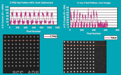
Figure 1. The multiple optical elements and bulky configurations of image intensifiers not only make x-ray sensors larger, but also can introduce distortion into the image. An x-ray image of a ball grid array test pattern was acquired for each imaging device using a Hamamatsu microfocus x-ray source. It was set to 40 kV peak tube voltage and 40 μA.
Early digital x-ray systems coupled CCD cameras to image intensifiers equipped with CsI photocathodes that provided good detection efficiency for x-rays above 10 kV. The bulky conversion and amplification elements in these intensifiers, however, required a large area on a lab bench (or inspection machine) and didn’t lend themselves to in-line inspection applications. Also, the number of elements in an image intensifier introduces mild image distortion, which is more noticeable near the edges (Figure 1).
Recently, flatbed x-ray scanners have emerged in much smaller packages and footprints, comparable to a videocassette. Their control unit dimensions follow suit, taking up little more space than a standard VCR. Combined, these trends are producing x-ray sources and sensor elements that more easily integrate into in-line inspection arrangements.
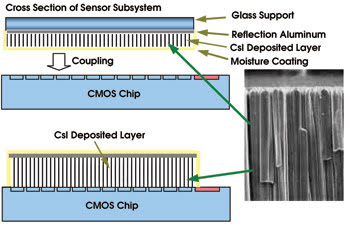
Figure 2. Flat panel x-ray scanners apply different scintillator materials in one of several configurations. This cross section of two scanners illustrates direct deposition of a CsI scintillator onto the detector’s surface, and flipped scintillator plates applying a CsI onto a glass plate that is flipped over a CMOS imager.
These scanners apply different scintillator materials in one of several configurations (Figure 2):
• Direct deposition applies a scintillator — usually CsI — directly onto the detector’s surface. This provides clear images but offers little protection against the x-ray radiation, reducing sensor lifetime. Direct deposition is better suited for medical imaging applications where the x-ray energies are considerably lower.
• Flipped scintillator plates apply CsI onto a glass plate that is flipped over a CMOS imager. The glass improves durability but can reduce the resolution and the low energy sensitivity.
• Structured scintillators, which confine light emitted by absorbed x-rays to narrow channels, are deposited on a fiber faceplate. The scintillator can be CsI crystals that have a needle structure and produce a high-resolution image or amorphous GdO2S, which is lower in cost and resolution. In either case, these gaps deliver the converted light directly to the sensor’s pixels, rendering excellent images and durable sensors. The drawback is that these screens often entail complex, costly manufacturing methods.
Figure 3 shows a performance comparison of the configurations.
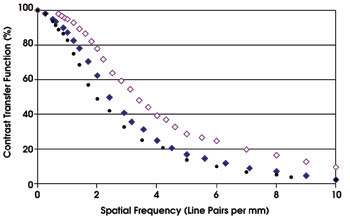
Figure 3. The resolution of an x-ray flat panel is determined by the type of scintillator material used. This graph displays the resolution of a sensor with 50-μm square pixels, using a directly deposited CsI material (purple), a CsI flipped scintillator plate (blue) and a GdO2S screen (black).
CMOS solutions
Amorphous silicon plates measuring 100 × 100 mm were considered as an alternative to CCDs. Their expansive area enables faster scanning over large areas, and the material also provides higher sensitivity. Unfortunately, these advantages come at a relatively higher price. CMOS technology is a more viable option because it offers performance comparable to CCD sensors and amorphous silicon, but often at a lower cost.
CMOS chips can be active or passive. Active chips incorporate microamplifiers into individual pixels, whereas passive chips amplify signals at the end of each column. Although active CMOS chips provide less image noise, passive chips are better suited for industrial inspection applications. For example, the absence of an amplifier in each pixel allows higher fill factors and, thus, chips with higher sensitivity. It also results in better uniformity because there are fewer gain variations from pixel to pixel. Lastly, passive chips have longer lifetimes because their amplifier element is not exposed to x-ray radiation.
Besides its relatively lower cost, CMOS technology’s single-chip architecture integrates a large 12 × 12-cm active area developed from a single 300-mm wafer that has pixels measuring 50 × 50 μm. This kind of resolving power is particularly useful for failure analysis but can be a hindrance in many applications that put equal or greater emphasis on throughput, such as semiconductor wafer processing and electronics manufacturing.
For these and similar applications, CMOS chips’ pixel binning capability allows them to read single 100-μm square pixels or 4 × 4 units measuring 400 μm. Read singly, CMOS pixels provide high eight-line-pair resolution. Binned pixels reduce resolution but increase frame rate up to 30 fps.
As with CCDs, the readout configuration of CMOS sensors can be dynamically adjusted so that the imager can rapidly scan large areas at low resolution and, if necessary, zoom in on suspect areas and switch to high-resolution pixel mode. For some applications, this flexible approach enables use of a single instrument for macro- and microinspection.
The largest commercial CMOS imaging chips, measuring 18 × 22 cm, are truly advantageous in large-area scan applications. The alternative is to collect images from two or more juxtaposed chips and to use software to stitch their separate images into a coherent whole. Besides compromising image quality, this complicates the data-processing step.
Real value
As focal spots of sealed x-ray sources diminish to 5 μm, these durable instruments expose flaws with greater resolution and clarity. Concurrently, CMOS technology has enabled flat panel sensors to resolve defects that are exposed by smaller focal spots. Where necessary, pixel binning offers the option to dynamically switch between high-resolution inspection and rapid large-area scanning.
Further design innovations in both source and detector configurations have reduced the dimensions, complexity and potential cost of these components. This not only facilitates their integration into in-line, automatic inspection operations, but also contributes to their ease of use.
These advances emphasize the value of microfocus x-ray technology for inspection of electronics, turbine blades and cast parts. But they will also fuel interest in new applications and markets where industrial nondestructive testing is essential.
Meet the author
John Gilmore is product manager of solid-state image sensors at Hamamatsu Corp. in Bridgewater, N.J.; e-mail: [email protected].