Clifford M. Krowne, US Naval Research Laboratory
The ability of left-handed materials to focus electromagnetic waves in unusual ways promises unique applications in subwavelength optical imaging and in radar. Now, as these materials make the transition from nearly 40 years of theory to reality, scientists worldwide are investigating their poten-tial uses across the electromagnetic spectrum.
One of the unusual properties of left-handed materials, when used with right-handed materials, is the ability to take diverging or parallel rays of light and to focus them with a flat plate of left-handed material. Definitive proof of such negative indices of refraction has emerged from several laboratories, and there is little question today that focusing possibilities exist in the much lower frequency microwave/millimeter regimes.
In ordinary matter, the energy flow, or power, is in the same direction as the phase front or phase motion of an electromagnetic wave propagating through it. The power flow of a wave is represented by the Poynting vector, P, and the phase front is represented by a vector describing the angular change per unit distance, k. At any given location P * k >0, where the dot indicates the multiplication of two vectors, called the dot product.
Left-handed materials, in contrast, do not produce positive dot products between the power and phase vectors. Rather, in these materials P * k <0, seemingly contradicting what we understand to be normal behavior.
However, there is nothing based upon Maxwell's equations that dictates that the product must be positive. Because it is known that the Poynting vector is equal to the cross product of the electric, E, and magnetic, H, fields, or P = E X H, in normal matter, it can be demonstrated that E, H and k form a right-handed system. If k points oppositely to P, the triad E, H and k must form a left-handed system. Indeed, this is how the term "left-handed materials" arose.
(It is important to note that measurements or simulations yielding a negative refraction angle provide a necessary condition for proving left-handed behavior. It is not a sufficient condition, however, because certain crystals or arrangements of crystals can be shown theoretically and experimentally to possess a negative refraction angle and yet are right-handed materials.)
Photonic crystals
Demonstrations of focusing using flat plates of left-handed materials or of negative refraction using left-handed prisms or wedges has been shown by simulation or laboratory experiment for waves at microwave to visible, photonic frequencies. Prisms composed of metamaterial lattices of split-ring resonator/metallic rod elements show a telltale sign of left-handed materials by producing negative refraction. Of course, power losses related to the metallic nature of these artificial lattices may be a problem in some of the frequency band regions in which one may wish to operate. As a result, it is important that there are alternatives to such assemblies.
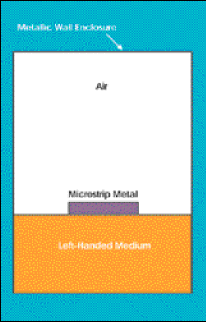
Figure 1. A cross section of a structure compatible with integrated circuits displays a left-handed substrate, a perfect conductor enclosing the device and a metal microstrip to provide the guided-wave mode (propagation perpendicular to the plane of the paper).
Some alternatives are suggested from the area of photonic crystals, in which lattices made of dielectric or metal inclusions of various shapes and arrangements can yield left-handed behavior. By creating defect regions, one can localize the energy to particular zones in an ordinary photonic crystal -- specifically, by using dielectric inclusions or voids. This has led to fiber optic applications, resonator or filtering possibilities in microwave circuits (using metal inclusions), and the exclusion of surface waves in substrates configured for microwave antennas (again using metal inclusions). Also, by investigating the band structure of infinite photonic lattices, regions of the ω-vs.-k space can be found that display the basic properties of left-handed materials.

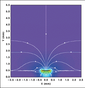
Figure 2. This diagram is a magnitude plot of the electric field distribution at 5 GHz, with an overlaid line plot giving the electric field vector. The solid black line at Y = 0.5 mm is the metal microstrip atop the left-handed substrate, as indicated in Figure 1.
It is of interest to integrate optical and lower-frequency components so that one may gain the most from electron-based functioning circuit components and from optical-based components, which may take advantage of the special focusing abilities of left-handed lenses. Therefore, it is natural to inquire into the possibilities for understanding what left-handed materials do in the lower-frequency photonic regimes in which electron-based components operate. In contrast to the imaging and radar applications stemming from left-handed materials, potential applications in electronics also may exist because new physics of propagation in left-handed materials occur in structures compatible with integrated circuits (Figure 1).
Treating the left-handed material as intrinsic with microscopic properties that may be described by constitutive relations relating the displacement field or electric flux density D and electric field intensity E, D = εE, and relating the magnetic flux density B to magnetic field intensity H, B = µH, enables one to study the electromagnetic fields within the guided wave structures that are employed in integrated circuits. One can obtain isotropic left-handed behavior if ε and µ above have physical properties that are consistent with ε <0 and µ <0, respectively, in some frequency band.
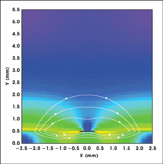
Figure 3. This diagram is a magnitude plot of the magnetic field distribution at 5 GHz, with an overlaid line plot giving the magnetic field. The solid black line at Y = 0.5 mm is the metal microstrip.
Forward, backward waves
Completely new dispersion diagrams (ω vs. k) and electromagnetic field configurations have been found (Figures 2 to 4).1,2 It has been proved that propagation in these structures enables regions of forward and backward waves to exist. Such new propagation behavior is in agreement with recent macroscopic realizations using lumped/distributed circuit elements to make backward-wave circuits.3
The use of left-handed materials in the construction of components for electronic devices is a relatively new field of inquiry in the study of these materials. Numerous microwave applications exist, including the use of left-handed materials for transmission lines and couplers, and other circuit elements with different or improved characteristics may be made. One could make new filters, for example, taking advantage of the propagation and evanescent frequency bands that exist in the dispersion diagram of microwave left-handed transmission lines.
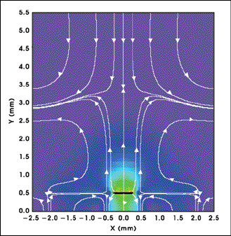
Figure 4. The magnitude plot of the electric field E distribution at 40 GHz shows an overlaid line plot giving the electric field vector. The solid black line at Y = 0.5 mm is the metal microstrip.
Additionally, the new electromagnetic field distributions strongly imply that improved isolators and circulators could be constructed using left-handed materials in combination with nonreciprocal materials based on carrier cyclotron motion or spin precession. New control components using reciprocal media are also possible by teaming up left-handed materials with ferroelectric materials, for example.