Austin Richards, Flir Systems, Indigo Operations
Jon Lesniak, Stress Photonics
Gavin Horn, University of Illinois
Silicon wafers are the fundamental building blocks of the microelectronics industry. The size of those used in fabricating integrated circuits has steadily increased because larger wafers yield more parts per processing step. As wafers grow to 300 mm in diameter and beyond, they become increasingly fragile and prone to stress buildup during manufacture.
Residual stress accumulates during the growth, sawing, lapping/grinding, etching and polishing operations before the wafer has even begun the processing stages necessary for integrated circuit manufacture. Cracks may be generated throughout processing, and if undetected, the wafers that survive can be rendered unusable in subsequent manufacturing stages. By using a camera-based imaging system to inspect the wafer throughout production, stress and cracking can be found before significant value has been added.
Stress Photonics Inc. of Madison, Wis., has developed an instrument that can visualize stress patterns in silicon wafers and devices with a high degree of clarity. The device illuminates the sample with broadband, circularly polarized near-infrared light. As light propagates through the silicon, residual stress-induced birefringence changes it from circular to elliptically polarized. Birefringence is a phenomenon whereby the speed of light in a transparent material depends on the orientation of the lightwaves' electric field. The resulting phase shifts affect the polarization state of transmitted lightwaves.
A polarizer rotating in front of the Alpha NIR InGaAs camera from Flir Systems, Indigo Operations, in Goleta, Calif., measures the ellipticity of the light received by each pixel. As the rotating polarizer aligns with the long axis of the ellipse, the pixel gets brighter, but as it aligns with the short axis, the pixel gets darker, creating a "flashing" effect. The magnitude of this flashing determines the stress measured by a particular pixel, and its phase indicates the orientation of the stress. Real-time, solid-state systems that measure the ellipticity without rotating polarizers also have been developed.
Stress Photonics has used this technology with visible light for quality control of automotive glass products for years, but it recently contracted with the National Science Foundation to collaborate with the University of Illinois at Urbana-Champaign to transfer this novel approach to the quality control of silicon products. Researchers at the university have successfully applied the system to the inspection of silicon wafers and microelectromechanical systems and bonded semiconductor devices. Because stress distribution is often at least an order of magnitude larger than the defects themselves, the stress caused by flaws of submicron dimensions can be imaged at much lower magnification than that necessary to find the flaw itself.
Stress patterns
A crack that is only a few millimeters long is difficult to see when the wafer surface is illuminated with a flashlight at an oblique angle, even under high magnification. Manual inspection is slow, operator-intensive and subject to human error. By measuring the transmitted infrared light intensity field, the crack is more apparent because of reflective losses at the crack faces (see figure, left).
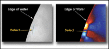
A crack, only a few millimeters long, is visible to the eye using traditional near-IR transmission imaging (left). Polarized near-IR stress analysis enables visualization of the defect from both the front and back sides of the wafer (right).
However, the stress patterns generated by the crack are even more visible in the polarized near-IR view with the stress analysis instrument (see figure, right). False coloration of the image indicates the ellipticity of transmitted light, which is proportional to the stress. Further inspection of similar wafers indicated that large residual stress had built up at the edge of this batch of wafers and may have been responsible for the damage that was occurring.
This inspection system, which provides both images (transmission- and stress-based) can be used not only to sort damaged wafers for quality control, but also to confirm the effects of process controls to indicate whether drift in this setting has affected the residual stress distribution.
The near-IR camera's InGaAs sensor operates in the 900- to 1700-nm region of the spectrum, well past the silicon cutoff. The camera generates 12-bit digital image data at 30 fps, which is transmitted via the low-voltage differential signaling standard to a frame grabber board in the PCI bus of the host PC. Controlled via an RS-232 interface, it is compact enough to integrate into a machine vision system. External triggering can be used to synchronize the camera with motion control systems and positioners that handle the wafer.
By employing broad-field illumination and the near-IR camera, as opposed to a laser source and a single photodetector, specimens with very rough surfaces can be inspected quickly and conveniently from the earliest stage of production through metallization. A higher wafer throughput also can be achieved, making 100 percent online inspection at rates of up to 30 fps a distinct possibility for many applications.