Typically considered competitive technologies, CMOS and CCD sensors have more in common than meets the eye.
Hank Hogan,Contributing Editor
Howard Rhodes, director of imaging engineering at Boise, Idaho-based Micron Technology Inc., is a proponent of CMOS sensors. That’s to be expected, given that the company is one of the largest manufacturers of CMOS imagers in the world. It is heavily committed to the technology and the resulting products. But Rhodes bases his support of CMOS on more than just company loyalty. He invokes physics and semiconductor device engineering, noting that both CMOS sensors and their main competitors, CCDs, are fabricated of silicon.
CMOS image sensors, like microprocessors and memories, are fabricated with specialized tools to create circuitry and photosensors on wafers. Courtesy of Tower Semiconductor Ltd.
“From this aspect, there is no difference, in my opinion, between CCD and CMOS. So CMOS should be able to achieve CCD performance, and we believe we have,” Rhodes said, adding that this equivalence has been demonstrated in laboratory settings and with prototype devices. CMOS products of comparable capabilities should be commercially available soon.
A look at recent developments from Micron, as well as from competitors Foveon Inc. of Santa Rosa, Calif., and Eastman Kodak Co. of Rochester, N.Y., shows that this equality may indeed be looming. Interesting innovations also are coming out of niche sensor supplier Sarnoff Corp. of Princeton, N.J., CMOS image sensor foundry Tower Semiconductor Ltd. of Migdal Haemek, Israel, and Belgium-based large-sensor maker FillFactory NV.
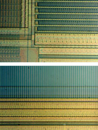
CMOS image sensors can have staggered pixels in an array (top), or the layout can be linear (bottom). Courtesy of FillFactory NV.
Smaller and smaller
According to market analysis firm Gartner Dataquest, wireless communications and consumer electronics will account for more than 60 percent of the $1.98 billion worth of CMOS sensors purchased in 2004. For camera-equipped cell phones and digital still camera applications, the drive is for more and more pixels in the same form factor. So sensor pixels are getting smaller.
That’s one area where CCDs have an advantage. Various CMOS manufacturers report that CCD sensors are shipping with 2.5-μm pixel sizes and sampling down to 2.2 μm. Those figures are well below the more than 3 μm of commercial CMOS sensors.
CMOS vendors are trying to catch up. Devices with pixels well below 3 μm have been demonstrated, but some optical problems must be solved before these smaller pixels appear in cameras. The first of these challenges arises because pixels aren’t just two-dimensional structures. They also have height. Insulating layers and conductive metals separate the active sensing element from color-discriminating microfilters and focusing optics. This third dimension causes problems as pixels shrink in the other two.
“To maintain the same optical performance, you actually need to bring the microlenses down closer to the sensor surface,” explained Cliff Drowley, director of the CMOS image sensor technology line for Tower Semiconductor.
Vendors are solving these problems by reducing the height of the insulating layers about 15 to 20 percent. That brings the microlenses closer to the active sensing element and ensures that photons from a given microlens end up on the appropriate pixel and not on its neighbor. A penalty may have to be paid in terms of overall electrical performance of the circuit because shrinking the insulator thickness can reduce the maximum speed. Drowley said that this was usually not an issue and that the reduction in height could be achieved without an increase in cost.
Other vendors are implementing different tricks. Some are putting air pockets inside the insulating layers to improve the optical transmission and reduce absorption. Others are tweaking the physical design of the pixel.
Although these efforts have been successful, clever engineering is running up against a basic optical problem. A smaller pixel covers less area, and less area means that fewer photons are captured. This is a problem that confronts any sensor, no matter what technology it’s based on.
“As you’re shrinking that pixel, the image is getting worse and worse,” said Richard Turner, vice president of product marketing at Foveon. “You get to a point where the only thing you are doing is increasing the megapixel number on your box. You are not increasing your resolution because, of course, there’s an optical limit.”
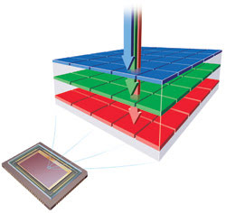
By exploiting the different depths, red, green and blue light penetrate silicon. X3 technology enables color capture without filters, allowing three pixels to be stacked. Courtesy of Foveon Inc.
Turner noted that, to get around this issue, Foveon depends on its proprietary X3 technology, which uses a triple well structure and exploits the different depths to which different wavelengths penetrate silicon. The company claims that this method effectively stacks three pixels into one piece of silicon real estate. It also contends that the technique offers color without filters and at triple the effective pixel density of more conventional approaches.
A parallel advantage
Then again, there are other ways to boost the active sensing area and improve the overall sensor fill factor, or the percentage of the light-sensitive area within a pixel. Some vendors are attacking the problem of smaller pixels by exploiting the parallel nature of the CMOS sensor architecture. By altering the design and layout, they can change the number of readout transistors needed to support a given pixel.
Herb Erhardt, technology manager for Kodak’s Image Sensor Solutions group, said that one arrangement of circuitry involved four transistors per pixel. Other circuit architectures can cut this figure substantially by sharing common transistors. In a scheme developed by Kodak, three of the four can service multiple pixels, allowing the number of transistors per pixel to drop from four to an equivalent of 1.75. This reduction offers a solution to the CMOS pixel size problem.
“We haven’t been able to scale the CMOS pixel as easily as a CCD one because we have three or four transistors in it. By applying the sharing concept, you can now begin realizing pixels that have reasonably good fill factors and that are beginning to approach the size of the smallest CCD. My guess is that, within the next year, you’ll see CMOS catch up to CCD,” Erhardt said.
Other advantages include a larger photodiode, better sensitivity, and either increased functionality or more storage capacity per pixel. The latter would allow a pixel to capture an image for a longer time or at a higher light level without saturating. A downside to the shared transistor approach is that it becomes more difficult to have an electronic shutter per pixel. Thus, doing something like flash photography with a shared transistor CMOS device may require a mechanical shutter.
Such shared devices and larger photodiode sizes also could be useful in other areas. Many machine vision and automotive uses of CMOS sensors don’t need color or can’t function with small pixel sizes. Pixels that measure 5 μm or larger are common for some of these applications. According to Curtis Stith, director of marketing for emerging markets in Micron’s imaging group, these pixels are larger for good reason. “Some of the requirements we face in industrial or, specifically, automotive use related to sensitivity drive you to a larger pixel,” he said.
Car sensors, for example, must work at temperature extremes and still produce usable images. For automotive applications, the device must work in low light and be able to transition to bright sunlight. The classic challenge is that of a car-mounted camera that must track features on a black road across a field of snow in bright sunshine. The shared transistor architecture and associated benefits could help solve this dynamic range problem.
The parallel nature of CMOS sensors also means that the technology lends itself to high-speed cameras. CMOS imagers can read out an entire row of pixels at once, instead of waiting for the serial transfer of charge that CCD sensors use. This ability is cited by John Tower, technical director for the imaging technology and products business unit of Sarnoff, as the reason why many high-speed cameras today are based on CMOS sensors.
Seeing scientifically
Tower noted that the parallel capability appeals to Sarnoff. The company is actively working on scientific-grade CMOS sensors, largely for the aerospace market. It has demonstrated a sensor that meets this description, and it has outlined the sensor’s performance at various scientific conferences and in publications. Results so far indicate a sensor noise level comparable to that found in CCDs. The similarity extends to more than just that performance aspect, however.
Tower, who described the new sensor as back-illuminated CMOS, said, “Just as you’d have back-illuminated CCDs for 100 percent fill factor and very high quantum efficiency, we’re working in the same direction for CMOS.”
He added that Sarnoff hopes to combine the high-speed, column parallel architecture found in CMOS with this higher level of sensitivity. The plan is to produce a high-speed imager suitable for either a standard or custom product within the next year. Some of the techniques developed could be put to use in other application-specific products.
It’s unclear how many, if any, of these innovations would be applicable to mass market offerings in the near term. However, large-volume applications would benefit from low-noise solutions. Smaller pixels mean less of a photon signal, and that makes a lower noise floor more important.
One of the techniques being implemented involves what are known as pinned photodiodes. As with back illumination, this method has been borrowed from CCDs and ported into CMOS. In a pinned photodiode, the sensing element’s potential is fixed relative to the device’s surface. The result is a sensor with very low noise and dark current.
Tower Semiconductor’s Drowley said that a pinned photodiode typically adds 5 to 15 percent to the production cost of a sensor wafer and requires a different pixel layout. The design change, however, allows the use of techniques that eliminate noise sources and image nonuniformities. In particular, it’s possible to remove time-dependent noise and reduce certain fixed-pattern noise. Those two sources contribute greatly to the overall degradation of the performance of a CMOS sensor.
It seems, then, that the two lines of sensor technology are converging in more ways than one, and that perhaps the two have silicon issues and solutions in common. As Drowley said of pinned photodiodes, “What we’re seeing in the market at small pixel sizes for the cell phone and digital still camera space is a move toward these types of structures with the better low-noise performance. It becomes very CCD-like as far as the photosensing element is concerned.
Acquiring the Right Image
The business of CMOS sensors is heating up. Analysts at the research firm Gartner Inc. in Stamford, Conn., project the 2004 market for CMOS imagers to grow 50 percent over last year. From 2003 to 2006, they forecast a 267 percent increase in CMOS imager market size and, by 2006, predict another surge of nearly 80 percent. That’s the year in which market analysts at iSuppli Corp. of El Segundo, Calif., predict a crossover, where CMOS sensor sales will exceed CCD sensor sales.
So a lot of CMOS sensors, chips and money will be made. Companies are preparing for what could be very good times. That explains, at least partly, the announcement in late June that San Jose, Calif.-based Cypress Semiconductor Corp. was acquiring FillFactory NV of Belgium for $100 million. In the deal, Cypress gets a company that makes some of the world’s largest and, in some ways, highest-performance CMOS sensors. For its part, FillFactory gets manufacturing muscle.
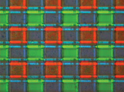
By overlaying the pixels in an array with a checkerboard of red, green and blue color filters, inherently monochrome CMOS sensors can capture a color image. Because the eye responds best to green, a popular approach devotes half of the array to sensing the green component. Courtesy of FillFactory NV.
“Up to this moment, we only used foundries. So we don’t have any in-house production capabilities, and that, of course, will change once we are part of Cypress,” said Lou Hermans, vice president of sales and marketing for FillFactory.
The expectation, Hermans explained, was that the company’s technology would be ported into Cypress’ CMOS factories for those products that could make use of state-of-the-art processing or that are aimed at high-volume markets. Prototyping of these new parts is under way, and plans call for full production of cell phone and digital camera sensors in 2005.
FillFactory’s existing customers and products will continue to be supported, and the company will still use foundries for some products, Hermans said. “These products are also mainly targeted to our niche markets. In a lot of cases, the risk and investment to move or to do the effort to transfer these products to a new process is too high.”
The acquisition also signals that others could be looking to move into the rapidly expanding CMOS imager market. That entry could come from companies already in the sensor arena.
Consider the case of the Rochester, N.Y.-based Eastman Kodak Co., which has a line of CCD imagers but has not had a large CMOS sensor footprint. Steve Noble, strategic marketing and business development manager for Kodak’s Image Sensor Solutions, said that the company has ongoing CMOS sensor research and development under way and hopes to have some new product announcements in the near future.