Just as tiny conductors "wire" electrons within an integrated circuit, optical waveguides written with femtosecond pulses soon will wire photons within integrated optical devices.
Rafael Gattass and Eric Mazur, Harvard University
Shortly after the invention of the laser, researchers discovered that intense laser pulses can cause dielectric breakdown and structural change in materials. This generally was considered a nuisance, hindering both research and the development of more powerful lasers.
In a paper on third-harmonic generation, Robert W. Terhune complained: "The experimental factor causing the greatest difficulty was breakdown or burning of the sample."1 Nicolaas Bloembergen referred to Terhune's complaint as he jokingly called the laser "the most expensive spark plug in automotive history."2 The development of more powerful lasers increased such accounts of laser-induced damage and led to a series of annual workshops known as the "Boulder Damage Symposia" that were devoted to the topic of "optical damage" caused by dielectric breakdown.
Theodore H. Maiman foreshadowed the use of the laser for cutting and welding in 1960, and the devices now are integral parts of many production plants, where they are employed extensively for the surface processing of absorbing materials.3 The use of laser-induced dielectric breakdown inside materials to create internal structural change, however, was not to come for several decades.
It is in this arena that lasers really stand out, as they offer a capability that no mechanical tool can: the processing of the bulk of a material without affecting its surface. Recent advances in this area of research make it possible to “wire light” from one point to another inside a transparent material, opening the door to the manufacture of monolithic, integrated optical circuitry.
Laser-induced optical breakdown is the process by which optical energy is transferred to a material, causing the ionization of a large number of electrons. These electrons, in turn, can cause permanent material modification by transferring energy to the lattice. In transparent materials, the energy of a single photon within the laser pulse cannot be absorbed (which is why they are transparent), so the material must simultaneously absorb more than one photon. For such nonlinear absorption to occur, the electric field strength in the laser pulse must be approximately equal to the electric field that binds the valence electrons in atoms.
To achieve such high electric field strengths, the light must be focused tightly. The tight focusing and the nonlinear nature of the absorption make it possible to confine the absorption to the focal volume inside the bulk of the material without causing any absorption at the surface. The result is a very localized deposition of energy in the interior of the sample. As the deposited energy is converted into thermal energy, the material can undergo a phase or structural modification, leaving behind a localized permanent change in index of refraction.
Ultrashort lasers
The advent of subpicosecond pulsed lasers in the late 1980s marked a turning point in the field of laser processing. Although pulses longer than a picosecond can cause optical breakdown, several problems mar the reliability and precision of laser materials processing with such pulses.4 First, to reach the threshold peak intensity for optical breakdown, a high pulse energy is required, but that causes the damage to extend beyond the focal volume. In contrast, subpicosecond pulses achieve the same peak intensity at much lower energy. The excitation then remains confined to the focal volume, making it possible to deposit energy with submicron precision.
Second, because the time it takes an excited electron to transfer the energy to the ions is on the order of a picosecond, thermal effects are not decoupled from the excitation. As a result, during the excitation of the electrons by the laser pulse, energy is transferred to the substrate, which causes the region around the focal spot to heat up.
Third, the occurrence of breakdown by long pulses tends to be random because the initial seed for breakdown is caused by impurities in the material. Subpicosecond pulses, on the other hand, generate the initial seed carrier density solely from multiphoton excitation. This gives rise to an extremely steady and fairly material-independent breakdown threshold.
The first measurements of surface damage thresholds of subpicosecond pulses in transparent materials were carried out in the mid-1990s at the University of Michigan in Ann Arbor and at Lawrence Livermore National Laboratory in Livermore, Calif.5,6 The goal of these measurements was to determine the dependence of the threshold for surface damage on pulse duration.
Shortly thereafter, in 1996, our group at Harvard University in Cambridge, Mass., and a group at Universität Essen in Germany reported vastly different results for damage thresholds when focusing subpicosecond pulses inside fused silica.7,8 Although the German group reported “clear evidence” that femtosecond laser pulses produced neither bulk plasmas nor bulk damage, we observed unmistakable evidence of bulk damage (Figure 1).
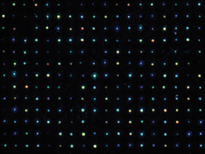
Figure 1. This differential interference contrast microscope image reveals an array of cavities written in quartz using a femtosecond laser. The coloration of the cavities is the result of interference between the light reflected at the front and at the back of each cavity. The spacing of the “voxels” is 2 μm. Photo by Felice Frankel.
The difference between these two experiments was in the focusing: We had used a microscope objective with a high numerical aperture, whereas the German group had used a lens with a low numerical aperture. The tight focusing provided by the high-NA objective minimized self-phase modulation and self-focusing outside the focal region and thereby maximized nonlinear absorption at the focus.
Our group proposed to use (and later patented) the internal microstructuring of transparent materials by ultrashort laser pulses for high-density, three-dimensional, binary data storage and for the micromachining of internal 3-D structures.9 We then set out to study the morphology of the damage and the mechanism causing the structural modifications.10
The same year, 1996, marked the first use of subpicosecond laser pulses for making waveguides by Kazuyuki Hirao’s group in Japan.11 Using amplified femtosecond pulses, the group demonstrated embedded optical waveguides in glass.
These first experiments led to an explosive growth in the processing of materials using femtosecond laser pulses. Within just a few years, femtosecond lasers were generally regarded as the pre-eminent tool for precise laser ablation.12 Optics conferences around the world soon began devoting sessions to “femtosecond laser micromachining.”
Micromachining
In 2001, our group demonstrated machining with femtosecond pulses of just nanojoules of energy, allowing machining to be done with a laser oscillator and eliminating the need for an amplifier.13 The key to lowering the energy threshold is very tight focusing: At numerical apertures above 1.0, the threshold energy drops below the pulse energy delivered by a typical femtosecond laser oscillator.
Using only an oscillator is fundamentally different from micromachining with amplified laser systems. Because the average output power is limited by the pump source, there is a trade-off between the pulse energy and the pulse repetition rate of femtosecond lasers. The interval between the pulses emitted by a femtosecond laser oscillator is on the order of tens of nanoseconds, which is significantly shorter than the 1-μs heat diffusion time out of the focal volume. Consequently, there is not enough time between successive pulses for the deposited energy to diffuse out of the focal volume.
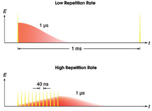
Figure 2. At a low repetition rate, the energy deposited by each laser pulse diffuses out of the focal volume before the next pulse arrives. At a high repetition rate, energy accumulates in the focal volume, making it possible to achieve very high temperatures around the focal volume with pulse energies of just a few nanojoules. Yellow indicates the laser pulses, red, the deposited energy.
Over time, the energy from successive pulses accumulates in and around the focal volume, producing damage (see Figure 2). The train of oscillator pulses constitutes a “point source of heat” at the focal volume within the bulk of the material. The longer the material is exposed to the train of pulses from an oscillator, the higher the temperature at the focus and the larger the region that is heated. If the temperature exceeds the material’s melting point, structural changes can occur. Chris B. Schaffer demonstrated melting and resolidification of material up to a radius of 50 μm.14
The pulses from an amplified femtosecond laser system, on the other hand, typically are separated by milliseconds. This far exceeds the time required for the generated heat to diffuse out of the focal volume, allowing the focal volume to return to room temperature before the next pulse arrives. Consequently, the structural change caused by an amplified laser is confined to the focal volume, regardless of the number of pulses that strike the sample.
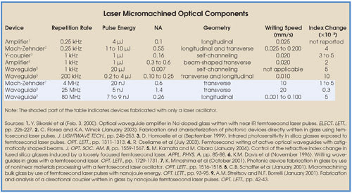 One of the most exciting applications of femtosecond micromachining of transparent materials involves the fabrication of three-dimensional waveguide structures — critical components for future integrated optical “chips.” Both femtosecond oscillators and amplified systems have been used to fabricate a number of simple devices, including beamsplitters, amplifiers and resonators (see table). The change in the index of refraction is roughly the same for writing at both low (amplified) and high (unamplified) repetition rates, although the gamut of materials used for low-repetition-rate machining (below 1 MHz, where pulse energy is not a limitation) is much larger. Waveguide writing also can be performed in several geometries using low repetition rates (Figure 3).
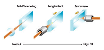
Figure 3. Different geometries may be used for micromachining waveguides in the bulk of transparent samples. The self-channeling and longitudinal geometries are usually used with amplified laser systems. Oscillator-only micromachining is performed transversely.
A simple, but limited, way to micromachine waveguides is to let nonlinear effects confine the femtosecond beam to a self-channeling filament. Typically, self-channeling is achieved with a lens of long focal length, and the micromachining occurs throughout the filament. Altering the focusing and the input power can control the waveguide dimensions. Because the resulting waveguide is necessarily straight, this geometry does not permit the micromachining of devices that include curves or bends.
Another widely used geometry is that of longitudinal irradiation: A long-working-distance objective with a fairly low numerical aperture focuses the beam inside the sample, which is translated parallel to the beam during irradiation. Because the waveguide is manufactured parallel to the irradiation direction, the diameter is defined by the transverse beam profile, making it possible to achieve fairly large core diameters.
Astigmatic lens
This technique also enables the fabrication of curves and bends, but the working distance of the objective limits the length of the waveguide. Transverse micromachining puts no limit on the length of the waveguide, but the cross section of the waveguide typically is elliptical because the structural modification is localized to the focal volume. To obtain a more spherical focal volume and to minimize the ellipticity, the laser beam can be shaped using an astigmatic lens.
In the case of high-repetition-rate, oscillator-only machining, the maximum pulse energy available restricts the choice of geometry. Usually, a high-numerical-aperture objective (NA ≥1) must be used, which necessitates a transverse writing geometry. The diameter of the waveguide is controlled by the translation speed of the sample: The slower the translation speed, the more pulses strike the same spot.
When more pulses strike the same spot, the radius to which the material is heated above the melting point increases and so does the diameter of the final waveguide structure. Because this diameter is determined by heat diffusion, the cross section of waveguides fabricated this way is nearly circular. The very high repetition rate of oscillators permits the fabrication of devices at writing speeds that are typically 100 to 1000 times higher than those obtained with amplified laser systems.
Toward application
The writing of internal waveguides makes it possible to wire optical breadboards, and the devices listed in the table comprise a basic tool chest of passive and active components for integrated optical circuits. The technique is a major step toward the realization of optical integrated circuits. Advantages of optical signal processing over electronic integration are the ability to connect in three dimensions and the lack of thermal energy dissipation. Femtosecond laser micromachining is a sequential process, however: Each circuit must be wired separately.
Oscillator-only micromachining relieves some of this limitation by making it possible to write at very high speeds. In addition, the past few years have seen the rapid development of smaller, simpler, cheaper and more powerful femtosecond laser oscillators. These developments greatly benefit waveguide writing with femtosecond lasers by providing greater control of the diameter of waveguides, increasing the speed at which devices can be made and broadening the range of materials that can be machined.
Waveguide writing with femtosecond lasers is well on its way to becoming the standard method for wiring light in integrated optical devices. It may be just a few years before an integrated optical device that is manufactured by femtosecond laser micromachining is used in a commercial application.
References
1. P.D. Maker et al (1963). Optical third harmonic generation. Proc. International Conference on Quantum Electronics, p. 1559.
2. N. Bloembergen (December 1997). A brief history of light breakdown. J. NONLINEAR OPT. PHYS. & MATERIALS, pp. 377-385.
3. T.H. Maiman (Aug. 6, 1960). Stimulated Optical Radiation in Ruby. NATURE, p. 493.
4. B.C. Stuart et al (March 20, 1995). Laser-induced damage in dielectrics with nanosecond to subpicosecond pulses. PHYS. REV. LETT., pp. 2248-2251.
5. D. Du et al (June 6, 1994). Laser-induced breakdown by impact ionization in SiO2 with pulse widths from 7 ns to 150 fs. APPL. PHYS. LETT., pp. 3071-3073.
6. Stuart et al, ibid.
7. E.N. Glezer et al (December 1996). Three-dimensional optical storage inside transparent materials. OPT. LETT., pp. 2023-2025.
8. D. von der Linde and H. Schüler (January 1996). Breakdown threshold and plasma formation in femtosecond laser-solid interaction. J. OPT. SOC. AM. B, pp. 216-222.
9. Glezer et al, ibid.
10. E.N. Glezer and E. Mazur (Aug. 18, 1997). Ultrafast-laser driven micro-explosions in transparent materials. APPL. PHYS. LETT., pp. 882-884.
11. K.M. Davis et al (November 1996). Writing waveguides in glass with a femtosecond laser. OPT. LETT., pp. 1729-1731.
12. X.B. Liu and G. Mourou (August 1997). Ultrashort laser pulses tackle precision machining. LASER FOCUS WORLD, p. 101.
13. C.B. Schaffer et al (January 2001). Micromachining bulk glass by use of femtosecond laser pulses with nanojoule energy. OPT. LETT., pp. 93-95.
14. Ibid.
Meet the authors
Rafael Gattass is a research assistant in Eric Mazur’s research group at Harvard University in Cambridge, Mass.; e-mail: [email protected]. Eric Mazur is Gordon McKay professor of applied physics and a professor of physics at Harvard University; e-mail: [email protected]. Together, they are working to develop new ways to wire light.