Producing photonic devices with standard silicon could revolutionize communications, computing, medicine and more.
Sean Koehl and Dr. Mario Paniccia, Intel Corp.
The siliconization of electronics over the past few decades has changed the face of the world. It has not only made what was once considered supercomputer-level computing readily available to almost anyone, it also has given us the ability to communicate through mobile phones, to document our lives with digital cameras, to enjoy feature films in which every frame is computer-generated, and to access information through the Internet at any time and from anywhere. Silicon chips are used in ways that no one dreamed of when the microprocessor was invented in 1968. The computing power that once occupied an entire room now fits into a chip the size of your fingertip. What, then, could the siliconization of photonics bring?
The number of photonic devices today that communicate data remains relatively low. Annual shipments of optical transceivers are measured in the millions. In comparison, the total number of computers shipped in one year is in the hundreds of millions. Considering that there are numerous connections within and between PCs and servers that are almost exclusively electrical, it becomes clear that well over 99 percent of the world’s interconnects remain copper-based rather than photonic (Figure 1). In addition, the cost of these copper connections in PCs is measured in pennies per pin versus hundreds of dollars per optical module in the long-haul and metro markets.
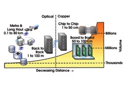
Figure 1. Optical interconnects are deployed today for long-distance, low-volume links. The vast majority of interconnects are still copper-based. There is a tremendous opportunity for photonics if components could be made in high volumes and at lower cost, enabling them to be used within and around PCs and servers.
With the continued advance of Moore’s law and the shift to multi- and many-core microprocessor architectures, bandwidth demands will continue to rise and push the limits of copper-based interconnects. Above 10 Gb/s, transmission over a copper line becomes challenging for all but the shortest chip-to-chip interconnects, and even these may not scale much beyond 20 Gb/s. This will force the maximum transmission distance to shrink, limiting architectures and exacerbating heat dissipation challenges by forcing hot processors closer and closer together.
A new way will be required to feed the data-hungry processors of the future. This is no small task. While we at Intel Corp. continue to research new methods to do this electrically, we are at the same time researching ways to use optical interconnects and technologies because of their tremendous data capacity, transmission distance and insensitivity to electromagnetic interference and crosstalk. However, because the entire optical industry is built upon volumes of less than 1 percent of its copper competitors, in its current state, photonics is simply not up to the challenge for cost-sensitive PC- and server-level links. New approaches, new technologies and major breakthroughs in photonics are needed.
A new contender
Enter silicon. The word is synonymous with abundant, low-cost computing power. Silicon integration and 40 years of driving Moore’s law have increased performance and lowered costs (Figure 2). In 1959, a discrete transistor cost about $6. Today, the same money spent on an integrated DRAM memory chip buys more than half a billion transistors.
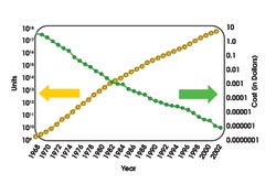
Figure 2. Moore’s law scaling has allowed the average transistor cost to drop dramatically with increasing volumes.
Certainly a silicon-based photonic device is a very different than a transistor. However, researchers at Intel’s Photonics Technology Lab realize that, if photonics could benefit even in a small way from silicon integration, photonics-based communication may prevail and unlock the true power of tomorrow’s computers and networks.
Only recently has silicon become a serious contender for producing photonic components. Detecting infrared light is tricky with silicon, and its lack of a significant electro-optic effect has made fast modulation and switching difficult. In addition, silicon’s indirect bandgap makes it a poor light emitter. Compound semiconductors such as indium phosphide and gallium arsenide, although expensive to process compared with silicon, have direct bandgaps that allow electrons excited by an applied voltage to release energy in the form of photons. Silicon’s indirect bandgap makes it far more likely that the energy will be released as heat, in the form of lattice vibrations. Although many university researchers are working hard to find creative ways to coax light out of silicon, none of these methods has been shown to be viable at the temperatures and powers required for real applications.
Light emission, however, is only one of many optical functions required by optical networks. Silicon has long been capable of optical transport and filtering, and recent research in silicon photonics has demonstrated significant performance improvements in the areas of switching, detection, modulation, wavelength conversion, amplification and even lasing. Moreover, silicon presents an attractive material for the monolithic integration of these functions. In more traditional photonic materials, such as indium phosphide, integration usually requires material regrowth steps that reduce manufacturing yields. As a result, very few commercial products today contain more than one device on a single chip — the electro-absorption modulated laser, a laser with an integrated modulator, being the only notable exception.
In addition, silicon has the benefit of billions of dollars in past and ongoing investments to advance Moore’s law. Some have called it the most studied material on Earth. The practical benefit is that, if photonic devices could be made using silicon wafers and the tools and facilities that were designed to make existing CMOS microelectronics wafers, the associated cost amortization would enable low costs. This could change the game, allowing photonics to ramp to high volumes for the mass market. As the silicon infrastructure continues to scale and mature, driving Moore’s law, silicon photonics would enjoy the ride.
Of course, the ride is not without obstacles. Producing compelling silicon photonic products in a CMOS fabrication facility presents a host of yet unsolved challenges in device performance, manufacturing, reliability and assembly.
History
Intel’s silicon photonics program has its roots in optical debugging tools developed in the late 1990s. At the time, Intel was starting to package microprocessors in a way that placed the silicon circuits face-down onto an organic substrate. The circuits became inaccessible to conventional electrical probing.
To provide continued access to the timing information of switching transistors, we developed an infrared laser voltage probe that, when directed though the back side of the silicon, interacted with the electrical current flowing across a transistor and modulated the laser beam. This tool eventually became an industry standard, and what we learned led us to explore using silicon for modulating and switching laser beams for optical communication.
The result was Intel’s gigahertz optical modulator described in the Feb. 12, 2004, issue of Nature, which used a device derived from a transistor to encode optical data more than 50 times faster than had been demonstrated in silicon. Because silicon lacks any appreciable electro-optic effect — used in materials such as lithium niobate for high-speed modulators — this was a giant step in silicon performance and a new building block for silicon-based photonics. The core device, which uses electrical charges to rapidly change the index of refraction in a silicon waveguide, can modulate, switch or even physically steer a beam’s direction. While we were developing this modulator, the project evolved into the larger silicon photonics program at Intel today.
Building blocks
Encoding data is only one of many building blocks that must be addressed to make silicon photonics relevant. To “siliconize” photonics, there are six main areas for investigation, including generating light, selectively guiding and transporting light within silicon, encoding light, detecting light, packaging devices and intelligently controlling all of these photonic functions.
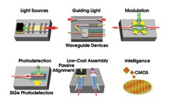
Figure 3. Six major building blocks are necessary to make silicon photonics communications a reality.
Light sources. Until a way is found to use silicon to convert electrical power into emitted photons, light generation will rely on an external component. The trick will be to use the cheapest infrared emitter possible and to treat it as an optical “power supply.” Silicon devices such as modulators, Raman lasers and/or filters may be employed to improve the quality or to manipulate the light as necessary. The source could be placed off-chip (attractive from a thermal perspective), attached to the silicon through passive alignment (see below) or mated directly to the silicon chip through techniques such as wafer-bonding. When communicating over relatively short distances (within a building, rack or server) a little bit of light goes a long way; one optical source potentially could power multiple devices on the silicon chip.
Along these lines, our laboratory has achieved major breakthroughs closely related to light emission. In early 2005, we demonstrated that, by using an effect called Raman scattering, we could amplify light and enable lasing within a silicon chip. As with the first laser, built by Theodore H. Maiman in 1960, this device uses optical rather than electrical energy for power. The silicon Raman laser can produce beams of coherent light with various unique properties.
Guiding light. Although opaque to visible light, silicon is transparent to wavelengths beyond about 1100 nm (Figure 4). This includes some of the more important communications wavelengths around 1310 and 1550 nm used to send high-speed data over telecom, metropolitan and some enterprise networks. Therefore, guiding and routing light within silicon waveguides is fairly straightforward.
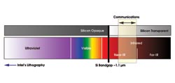
Figure 4. Silicon is transparent at the 1.3- to 1.6-μm communications wavelengths used today to send data long distances over fiber.
Silicon can be used to filter, split, bend or even multiplex multiple beams of different wavelengths. In this area, our laboratory has been particularly interested in creating filters to select or reflect individual wavelengths. Both thermally adjustable and thermally insensitive filters are under investigation to tune or stabilize lasers or to provide wavelength-selective building blocks. In addition, we work continually to reduce the optical loss and to improve the transmission properties of our waveguides.
Modulation. Modulation, the encoding of optical data, can be achieved simply by toggling the laser’s drive current or by sending it through another device that rapidly shutters the light. Our initial modulator was the first silicon device to modulate data at gigabit speeds. Since then, we have improved the device, and it has been used to transmit data at speeds of up to 10 Gb/s, in line with today’s high-speed communications needs.
The device consists of optical phase shifters embedded into optical waveguides that are built in the form of a Mach-Zehnder interferometer (Figure 5). The phase shifter — the key component — is essentially an electrical capacitor that can quickly bring charges into and out of the path of light. These electrons shift the phase of the light via the free-carrier plasma dispersion effect. The interferometer structure allows the phase shift to be converted into an amplitude modulation by canceling or adding the two interfering beams upon exiting the interferometer.
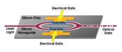
Figure 5. The silicon modulator works by directing light into a Mach-Zehnder interferometer containing fast silicon phase shifters. When toggled with complementary electrical data, the phase shifters determine whether the beams interfere constructively or destructively (add or subtract) when they recombine, resulting in optical ones and zeros.
Photodetection. Modulated data can be sent over an optical interconnect to another device a few centimeters, a few meters or a few kilometers away. When the signal arrives at the destination, the photons must be reconverted to electrons by a photodetector. The issue for silicon is that, because it is transparent at these infrared wavelengths, the light passes through without being absorbed. Silicon can detect visible light in a digital camera, but detecting infrared colors requires additional effort. To this end, our laboratory is looking into adding germanium to make silicon devices that absorb infrared light.
Germanium’s material properties allow it to detect light much farther into the infrared than silicon, and it is becoming available in many CMOS fabrication facilities. If germanium or a SiGe alloy is deposited on top of a silicon waveguide, light can be coupled into the layer and be absorbed.
The challenge is that the differences in the crystal structures of germanium and silicon lead to lattice defects when germanium is grown on silicon. These defects cause an undesirable noise called dark current — electrical currents generated even when no light is incident on the detector.
To date, Intel has achieved compelling results for the three principal photodiode metrics — dark current, sensitivity and bandwidth —when optimized independently. Research is focused on getting high performance at all three metrics in one device.
Low-cost assembly. For mature optical products today, packaging and assembly account for roughly one-third of the cost of the final product, because optical devices must be painstakingly actively aligned with the laser light on. Even today’s state-of-the-art active alignments are manual and complex and contribute significantly to cost.
To reach truly low costs at high volumes, optical fibers or any other external optical components (such as a light source) must be attached passively. Techniques to solve the alignment problems may include micromachining grooves and bumps into the silicon during fabrication. Alternatives may include the use of coupling structures called tapers that efficiently funnel light from fiber or a laser into a waveguide. We also are investigating methods of preparing the optical interfaces where light enters and exits the silicon by micromachining, smoothing and coating them at the wafer level before they leave the cleanroom.
Intelligence. Optical components still must be driven with, controlled by and interfaced to electronics. The silicon solution is simple: standard CMOS circuits. These electronic chips would be integrated with a device at the package level or attached directly to the silicon surface. Because the rule is to manufacture all devices in a CMOS fabrication, Intel has the opportunity to explore the pros and cons of monolithic optoelectronic integration of key devices, such as the circuits that convert photodetected currents into logic-level voltages. However, because the disparate processes could be better optimized individually, the hybrid attachment of electronic and photonic chips will be more cost-effective in the near term.
Future paths
The first phase of research has been to produce a compelling set of these optical building blocks. The silicon photonics research community has made significant advances in silicon device performance in recent years. Soon we will be able to begin the next phase, building “hybrid” assemblies for real applications. Starting with a silicon optical bench, in which electronics and photonics are passively aligned on a micromachined silicon assembly platform, researchers will begin to integrate certain functions directly into the silicon.
For instance, a silicon multiplexer and detectors could be integrated to form a multichannel receiver, or silicon modulators, lasers and passive components could be integrated to create a multichannel transmitter. This will happen only when the integrated solution brings a benefit to the final module, which may be increased performance, a smaller form factor or lower total cost.
Figure 6. In this concept of a future integrated transceiver, fibers are attached directly to the silicon.
The final phase of research will be to approach monolithic silicon integration (Figure 6). Components will be put together to form modules that process light in ways that could never be done before and at costs low enough to allow them to become ubiquitous. This will include photonic components — possibly even the light source (if there is a breakthrough in silicon emitters) — and electronics. Again, the level of monolithic integration will be determined by economics.
Many challenges must be addressed to make integration a reality, and some are less obvious than others. These include thin-film topology for the relatively large waveguides, contamination of the factory with new materials, optical metrology, tolerance to heat dissipation, process complexity and thermal budgets. In-line testing is a major practical issue. The tools that exist to measure important optical parameters, such as index of refraction, do not exist in microelectronic fabs. Wafer-level testing is essential for high yields in the electronics industry but is extremely challenging for planar photonic devices. Creative methods for vertical coupling or integrating monitor photodiodes must be developed. These and other issues must be studied and solved to produce high-yielding, low-cost, silicon photonic products.
Silicon photonic chips could dramatically change the way that enterprises use photonic links for their systems and networks. The option to use photonics could eliminate bandwidth and distance limitations, allowing for radically new and flexible architectures capable of processing data more efficiently.
There also will be applications beyond digital communications, such as sending analog radio signals over fiber to distant locations, making the distribution of wireless signals cheaper by eliminating the need for a digital-to-analog conversion at the end point. Rack-size telecom routers could be reduced to an integrated chip that includes silicon switches derived from the same core technology that is used to build silicon modulators.
Intel’s silicon laser, as with other Raman lasers sold today, has the advantage of shifting a wavelength further into the infrared — even into regions that semiconductor lasers do not access. This could have uses for some spectroscopic and biotechnical applications that require mid-infrared wavelengths — and bulky crystal lasers to reach them. Furthermore, because the Raman scattering is not tied to a bandgap, a silicon laser can lase at any wavelength for which silicon is transparent (above about 1100 nm). If successful, silicon photonics could revolutionize medicine by replacing multiple tabletop lasers with a compact, tunable silicon laser.
Integrating silicon photonics with microfluidic channels etched into silicon could enable “lab on a chip” devices in which proteins or DNA strands flow past a beam of light, which then would be filtered and detected. As researchers unlock the mysteries of the genetic code, low-cost devices such as these could lead to the early detection and monitoring of diseases. Silicon could make widespread the use of optical sensors to analyze and monitor chemicals in the environment around us.
Most importantly, as with electronics, the availability of low-cost, integrated devices will empower people to use photonics in ways we can’t imagine today. Building photonics in silicon would be revolutionary, with a tremendous return.
Silicon solution
Because of the relentless push of Moore’s law, microprocessor performance will continue to rise, and the cost of each additional MIPS (million instructions per second) will continue to drop dramatically. Application designers will use that increased performance to improve the user experience, creating intelligent, aware systems that react to the environment and that anticipate our needs. Wireless networks will enable a new generation of digital media devices whose users will stream a crushing tide of video and audio to a billion screens.
Computers and networks will be hit with a veritable tsunami of data. The bottleneck will be the electrical connections between computers and chips.
Our lab is betting that silicon photonics will be the solution.
For more information, please visit www.intel.com/go/sp.
Meet the authors
Sean Koehl is senior technical marketing engineer for silicon photonics, and Mario Paniccia is director of the Photonics Technology Lab, both at Intel Corp. in Santa Clara, Calif.; e-mail: [email protected].