Investigators pursue both electrical and optical pumping of silicon lasers.
Dr. Bahram Jalali and Sasan Fathpour, University of California,
Los Angeles
Compound semiconductors have long been the workhorse for light generation and amplification in optoelectronic devices, whereas silicon has been the de facto standard for electronic integrated circuits. Driven by the material’s cost advantage, creating optoelectronic devices in silicon has been a subject of intense research. Such a technology, called silicon-based photonics, would be compatible with electronic integrated circuit and microelectromechanical systems (MEMS) technologies. It could usher in sophisticated multifunctional chips on which electronics, optics and MEMS would be synergistically combined.
Among the family of photonic devices, light emitters (LEDs and lasers) have been the most challenging to obtain. This has to do with bulk crystalline silicon being an indirect bandgap material, which means that the upper and the lower electronic states (conduction and valence bands) do not have the same value of momentum (Figure 1). Because the photon of interest has negligible momentum compared with that of the electron, the electron-hole recombination must be mediated by emitting or absorbing a phonon to conserve momentum. In the terminology of quantum mechanics, this is a second-order process, which implies that, although not forbidden, the probability of occurrence is extremely low. Such radiative recombination events are rare, being characterized by a very long lifetime on the order of 1 s.
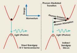
Figure 1. In a direct bandgap material such as GaAs, electrons in the conduction band recombine with the holes in the valence band, transferring their energies to emitted photons. In an indirect bandgap material such as silicon, the recombination is mediated by absorption or emission of a phonon. This is much less likely than a competing event that involves defects and impurities and that is nonradiative.
On the other hand, the experimentally measured lifetime in silicon is in the millisecond to microsecond range, depending on the impurity or defect concentration. This suggests that radiative processes in silicon are insignificant, and that experimentally observed recombination occurs through impurities or defects. Such processes are nonradiative, where the energy is eventually dissipated as heat.
A useful metric is the electron-to-photon conversion efficiency, given by the ratio of the nonradiative lifetime to the total lifetime. This computes to an efficiency of 10–3 to 10–6 for bulk silicon. In contrast, in direct bandgap III-V semiconductors, where momentum is readily conserved during recombination, the radiative lifetime is orders of magnitude lower. The radiative process is so fast that, in a good quality crystal, defect- or impurity-assisted nonradiative processes cannot compete with it. This leads to a conversion efficiency that is close to unity for a material such as GaAs.
LEDs that are fabricated in bulk silicon typically use high-purity silicon and realize an electrical-to-optical conversion efficiency of 10–4 to 10–3. Researchers at the University of New South Wales in Sydney, Australia, reported a relatively high conversion efficiency of around 1 percent for such devices.1 They also reported that the enhancement resulted from the passivation of the silicon surface that leads to a reduction in nonradiative recombination through surface states, and that the texturing of the silicon surface further improved efficiency.
Despite relatively high-efficiency improvement in this approach, optical amplifiers or lasers have not been obtained. The reason is that, because of the very low radiative rate in bulk silicon, extremely high carrier concentrations are needed to obtain a population inversion. The high carrier concentrations cause Auger recombination and free-carrier absorption, which will prevent laser operation. The situation would be different if one could break free of the low radiative rate of bulk silicon.
The successful realization of optical amplification in Er-doped optical fiber has motivated efforts to achieve light emission using erbium in silicon. In fact, the atomiclike transition energy of erbium ions corresponds to a wavelength of 1.54 μm; i.e., a standard telecommunication wavelength. Unlike the case of luminescence in Er-doped glass — which is caused by resonant absorption of pump photons — erbium emission in silicon is a carrier-mediated process via optically generated electron and hole pairs, otherwise known as excitons (Figure 2).
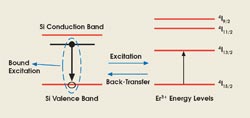
Figure 2. The trapped electrons in Er-related deep levels within the silicon bandgap form a bound exciton (an electron-hole pair tied together by Columbic interaction resembling a hydrogen atom). Exciton recombination can excite the 4f-shell levels of the Er3+ ion. Finally, the excited Er ion can decay radiatively, emitting light at a wavelength of 1.54 μm.
Electroluminescence from Er-doped silicon at 300 K was demonstrated about a decade ago. However, the intensity decreases significantly when the temperature is increased from ~100 K to 300 K. Possible explanations for the degradation are dissociation of excitons at high temperatures and the back-transfer of carriers from the excited erbium ions to the trap states.
Quantum confinement is another approach to overcoming the inherent luminescence inefficiency of bulk silicon. According to the uncertainty principle, carriers confined within a region of length Δx experience a momentum ambiguity of Δp ≈ h/Δx (h is Planck’s constant). In other words, the probability of radiative recombination increases because the momentum conservation condition is relaxed.
Early efforts concentrated on porous silicon, which produces luminescence at room temperature in the visible spectrum. Its drawback is the high reactivity of the spongy texture of the material, which causes severe reproducibility and reliability problems for the LEDs.
A more viable technique to create quantum confinement is to produce nanocrystals in a silica matrix. Compared with porous silicon, silicon nanocrystals benefit from the stability and high quality of the Si/SiO2 interface. The most widely used techniques to create nanocrystals are ion implantation of silicon into ultrapure quartz substrates and the deposition of thin silica films with a large excess of silicon. Typically, the nanocrystals are ~3 nm in diameter and form with a volume density of ~2 × 10¹⁹/cm3. Recombination facilitated by electronic energy levels that exist at the interface between silicon nanocrystals and SiO2 (surface states) plays an important role in the emission properties. The emission spectrum has a broad peak centered at 800 nm.
Because the nanocrystals are hosted in an insulating material (SiO2), utilizing a PN junction is not possible, and metal oxide semiconductor (MOS) structures have been the configuration of choice to demonstrate light-emitting devices. Excitation of silicon nanocrystals is believed to be through the impact of hot electrons created by direct tunnelling into nanocrystals. By increasing the nanocrystal density, the operating voltage of the device is reduced, and the total efficiency increased. Therefore, despite difficulties of direct injection of carriers into nanocrystals, reasonably strong room-temperature luminescence with an intensity peak at 850 nm has been reported with voltages as low as 4 V.2
De-excitation caused by the back-transfer of energy from excited erbium ions to silicon, shown in Figure 2, reduces the efficiency of Er-doped LEDs. The problem can be alleviated considerably if erbium dopants are coupled into nanocrystals embedded in a SiO2 matrix. Quantum confinement increases the effective bandgap of silicon, resulting in the efficient pumping of erbium into its higher states by the excited nanocrystal. This is followed by rapid relaxation into the first excited state ( 4I13/2 ), from which the radiative transition at 1.54 μm to the ground state can occur.
The increase in the effective energy bandgap in silicon nanocrystals increases the mismatch between erbium and silicon, reducing the efficiency of the back-transfer. Nanocrystals act as sensitizers for erbium ions, improving their pumping efficiency by several orders of magnitude. They also allow erbium to be pumped with low cost LEDs. Electroluminescence at 1.54 μm with a quantum efficiency of ~1 percent at room temperature has been demonstrated in MOS-type LEDs.3
Amplification in silicon was first reported in nanocrystal-doped SiO2 at 800 nm.4 However, for applications to silicon photonics, wavelengths larger than 1100 nm are desired because silicon is opaque below this wavelength.
Recently, a gain value of 0.7 cm–1 at 1535 nm was reported in nanocrystal/Er-doped SiO2 waveguides.5 To assess the prospect for a laser, it is instructive to compare this value with that of an established technology such as InAs quantum dots. The III-V nanostructure technology has produced lasers with record-low threshold currents. The gain value of InAs quantum dots is typically about 5 cm–1 per quantum-dot layer, and it is <30 cm–1 in multilayer quantum-dot lasers. Clearly, the gain in the erbium/nanocrystal is not competitive with InAs technology at this time.
Although there has been a report of electrically pumped stimulated emission in PN junctions (formed by using boron dopant mixed with SiO2 nanoparticles),6 the SiO2 film doped with erbium and nanocrystals has been the most commonly pursued approach to electrically pumped silicon lasers. However, several important challenges remain before lasing can be expected.
The first has to do with the MOS-type devices employed for electrical pumping. It is not clear whether tunneling through the oxide can provide the high current densities required for lasing. The highest current density reported is ~30 A/cm2, which is about an order of magnitude lower than typical currents in InAs quantum-dot lasers. Another significant challenge will be achieving a waveguide with large optical confinement that also is electrically conductive. In other words, a conductive cladding layer for the Er-nanocrystal-doped SiO2 is necessary. Auger recombination and free-carrier absorption will pose additional challenges.
So far, Raman scattering has been the only approach capable of achieving lasing in silicon. Raman scattering has long been exploited in optical fibers to create amplifiers and lasers. However, several kilometers of fiber typically are required to create a useful device. Often overlooked was the fact that the gain coefficient for stimulated Raman scattering in silicon is approximately 103 to 104 times higher than that in silica fiber. Additionally, silicon waveguides can confine the optical field to an area that is approximately 100 times smaller than the modal area in a standard single-mode optical fiber.
When combined, these facts make it possible to observe stimulated Raman scattering over the interaction lengths encountered on a chip. This was validated through experimental demonstration of spontaneous and stimulated Raman scattering in silicon waveguides.7,8
The first silicon laser was demonstrated in 2004 and made use of the Raman effect.9 That work was followed by the demonstration of a continuous-wave Raman laser in 2005.10
The key to the success of the Raman approach is that it bypasses the problem of indirect bandgap in silicon. Although the microscopic description of Raman scattering in semiconductors is complex and beyond the scope of this article, there exists a much simpler macroscopic model that serves to explain the salient features of the phenomenon.
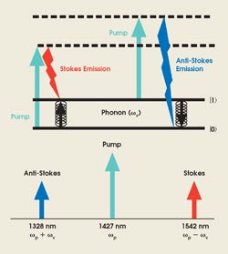
Figure 3. In stimulated Raman scattering, a pump photon elevates the system from a lower state into a (virtual) higher state. The system will then decay to a lower state by emitting a photon. If present, a secondary light beam at the Stokes frequency will be amplified. Also shown is the process of Raman-enabled four-wave mixing used for Stokes to anti-Stokes wavelength conversion.
In spontaneous scattering, thermal vibrations of crystal at frequency ωv (15.6 THz in silicon) produce a sinusoidal modulation of the optical susceptibility (the material’s transfer function). The incident pump beam produces an electric polarization that is given by the product of the susceptibility and the incident field. As illustrated in Figure 3, the beating of the incident field oscillation (ωp) with oscillation of the susceptibility (ωv) produces polarizations at the sum frequency ωp + ωv (anti-Stokes), and at the difference frequency ωp – ωv (Stokes). In the case of stimulated amplification, the interaction of the pump and Stokes waves produces a driving force for crystal vibrations and enhances the transfer of power from the pump to the Stokes wave, causing amplification at the Stokes frequency.
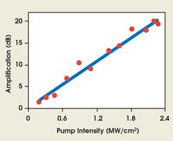
Figure 4. A maximum gain of 20 dB was obtained in a silicon optical waveguide using 30-ps, 20-MHz pump pulses.
Silicon is transparent at wavelengths above 1.1 μm. However, at the high pump intensities required for stimulated Raman scattering, two-photon absorption occurs. This itself is not a major detriment, but the free carriers that are generated create significant losses that can prevent lasing.
One approach to avoiding this problem is by using pulsed pumping. Figure 4 shows the measured Raman gain in a silicon optical waveguide when 30-ps, 20-MHz pump pulses are used. The input signal beam experiences a pump on-off amplification of 20 dB, clearly demonstrating the potential of the Raman approach in rendering silicon an optically active medium.
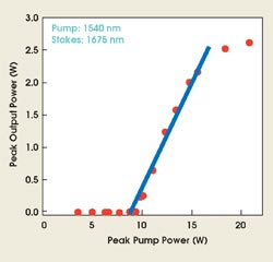
Figure 5. In the first silicon laser, the lasing threshold was measured to be at a peak pump pulse power of 9 W. The slope efficiency was approximately 34 percent. The laser produced output pulses with more than 2.5 W of peak power.
Figure 5 shows the transfer function of the first silicon Raman laser. The laser used a 1.7-cm-long silicon waveguide gain medium in an external-cavity configuration that was pumped by 30-ps, 20-MHz pulses. It had a slope efficiency of 34 percent and produced output pulses with more than 2.5 W of peak power. Other results also provided the first observation of anti-Stokes generation in any type of Raman laser, produced by parametric Raman conversion within the laser cavity. With a phase-matched and doubly resonant waveguide design, these lasers will be able to simultaneously produce significant output in two wavelength bands. In particular, if pumped at 1430 nm, the lasers will produce radiation at 1550 and 1320 nm, in the two most important communications bands.
In summary, optically pumped silicon lasers have been demonstrated using the Raman effect. The next milestone will be an electrically pumped laser. The erbium and nanocrystal-containing glass (silica) waveguide, pumped by a tunnel diode, is the most commonly pursued path toward an electrically pumped laser. Besides the low values of gain reported in this system, the other challenges will be achieving high enough injection current density into the insulator material and overcoming the lack of a conducting cladding layer. Auger recombination and free-carrier absorption will pose additional challenges.
References
1. M.A. Green et al (Aug. 23, 2001). Efficient silicon light-emitting diodes. NATURE, pp. 805-808.
2. G. Franzò et al (January 2002). Electroluminescence of silicon nanocrystals in MOS structures. APPL. PHYS. A, pp. 1-5.
3. F. Iacona et al (Oct. 21, 2002). Electroluminescence at 1.54 μm in Er-doped Si nanocluster-based devices. APPL. PHYS. LETT., pp. 3242-3244.
4. L. Pavesi et al (Nov. 23, 2000). Optical gain in silicon nanocrystals. NATURE, pp. 440-444.
5. J. Lee et al (January 2005). Optical gain at 1.5 μm in nanocrystal Si-sensitized Er-doped silica waveguide using top-pumping 470 nm LEDs. J. LIGHTWAVE TECHNOL., pp. 19-25.
6. M.J. Chen et al (March 22, 2004). Stimulated emission in a nanostructured silicon pn junction diode using current injection. APPL. PHYS. LETT., pp. 2163-2165.
7. R. Claps et al (Nov. 4, 2002). Observation of Raman emission in silicon waveguides at 1.54 μm. OPTICS EXPRESS, pp. 1305-1313.
8. R. Claps et al (July 28, 2003). Observation of stimulated Raman amplification in silicon waveguides. OPTICS EXPRESS, pp. 1731-1739.
9. O. Boyraz and B. Jalali (Oct. 18, 2004). Demonstration of a silicon Raman laser. OPTICS EXPRESS, pp. 5269-5273.
10. H. Rong et al (Feb. 17, 2005). A continuous-wave Raman silicon laser. NATURE, pp. 725-728.
Meet the authors
Bahram Jalali is a professor of electrical engineering and director of the Optoelectronic Circuits and Systems Laboratory at the University of California, Los Angeles; e-mail: [email protected]. Sasan Fathpour is a postdoctoral research scientist at the university; e-mail: [email protected].