Continuing to follow Moore’s law presents challenges for the photonics companies that serve the semiconductor industry.
Hank Hogan, Contributing Editor
For semiconductor makers, Moore’s law is more than an interesting observation of the rate of the doubling of transistor counts. It is the road map to commercial survival. The increase in functionality means smaller circuit features and lower costs per feature, key drivers for continued success.
For the photonics companies that serve the semiconductor industry, this doubling every 18 months defines the need to be able to resolve and measure ever-smaller features at an ever-shrinking cost. There are signs that it may be getting too hard to continue to pull off.
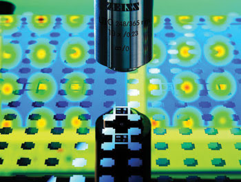
Lasers play a key role in checking and qualifying masks for semiconductor lithography. Courtesy of Carl Zeiss SMT AG.
“For the laser industry, we believe there are three axes that this challenge translates to,” said Sri Venkat, director of microelectronics marketing at Coherent Inc. of Santa Clara, Calif. “The first is the wavelength of the laser, the second is power, and the third is cost of ownership.” The task, he said, is to find the point at which the three are optimized for a given situation.
In semiconductor manufacturing, electronic circuits are built of alternating layers of conductors and insulators. Those materials and the semiconducting substrate are fashioned into the appropriate shapes, lines and spaces via lithography. Today that transfer is driven by light, with various wavelengths patterning the resist and illuminating the alignment of layers and the pattern integrity. Complementary detectors check the resulting features, with dimensions measured in nanometers.
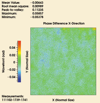
Phase-shift masks enable semiconductor manufacturers to print smaller features. That phase shift must be verified before the mask can be used. This plot shows the measured phase shift, obtained using an excimer laser. Reproducibility of phase measurement is 0.3 nm at a wavelength of 193 nm. Courtesy of Friedrich Alexander Universität Erlangen-Nürnberg.
Cymer Inc. makes excimer laser sources that power lithography scanners. According to Nigel Farrar, vice president of lithography applications marketing at the San Diego company, a consequence of Moore’s law shows up in what has happened to the output power divided by the spectral bandwidth of ArF excimer lasers over the past seven years.
“That metric has increased by a factor of 100,” he said. That essentially is a doubling per year.
This trend cannot continue forever. Constant doubling eventually would lead to power densities that would damage the optics of either the laser or the lithography tools. If the lifetime of the optics were degraded, the cost of the system would shoot up.
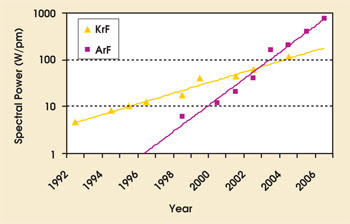
A consequence of Moore’s law for photonics is apparent in the trend of increasing spectral power from excimer lasers. The advances in power are unlikely to continue, as they eventually would yield additional expenses as a result of reduced component lifetime and increased system complexity. Courtesy of Cymer Inc.
Moreover, this hundredfold increase was possible in part because manufacturers moved from a single- to a dual-chamber laser solution. One chamber generates the narrow-bandwidth radiation needed, while the other amplifies the power. Extending this approach as a way to boost performance would add to the complexity and, again, to the cost of the scanner.
Addressing Moore’s law
There are various ways in which the problem of following Moore’s law may be solved. Extreme-ultraviolet lithography, employing 13.5-nm rather than today’s 193-nm state-of-the-art sources, is one possibility. Although considerable work must be done in terms of resist, sources and optics, the technology has attracted interest and research funding from Cymer and other vendors, as well as from chip makers such as Intel Corp. of Santa Clara and Advanced Microdevices Inc. of Sunnyvale, Calif.
The advent of EUV may still mean that deep-UV lasers will continue to be employed. One approach is to use the lasers to produce a plasma that generates EUV photons. Farrar said that his company believes such a strategy will allow the power of the EUV source to be scaled up to the level required to produce the needed scanner throughput.
There also are extensions of current optical lithography that may put off the time when EUV is necessary. The industry is deploying immersion scanners, in which the air gap between the tool and wafer is replaced by water. Using liquids other than water could continue that trend. Such techniques may allow for optics with a higher numerical aperture and, consequently, may enable lithography of smaller features. One challenge is finding a liquid with a higher refractive index than water that also has a low absorption at 193 nm.
Another optical extension involves a double exposure. The idea is that achieving the tight lines and spaces of a given layer may not be possible. However, exposure of half the pattern, followed by exposure of the other half, may yield satisfactory results. If such an approach is taken, the alignment and overlay of the half layers become critical.
Optical methods are preferred for alignment and overlay measurement, said Advanced Microdevices’ strategic lithography technology manager Harry Levinson. Such methods today make use of standard sources and detectors that operate from the red to the ultraviolet. However, there is a problem with the extremely precise measurements needed and the short depth of focus in standard microscopy.
“The people who build tools for overlay measurement often have to acquire the data in two passes, focusing first at the resist on top and then again focusing on the substrate, which, again, can even be somewhat buried inside the films under the resist,” Levinson said. Advances in microscopy, particularly those that extend depth of focus, could benefit these measurements.
Besides lithography, photonics plays a role in metrology, or the measurement of the parameters of interest, in semiconductors. One such parameter is feature size, and here a technique known as scatterometry is finding favor.
As the name implies, scatterometry analyzes the spectra of light scattered by a grating. In this case, the grating is composed of test lines and spaces created by lithography on a silicon wafer. Sweeping the wavelength of an interrogating beam from red to ultraviolet produces a scattered spectrum characteristic of the grating. From this, linewidth and feature profile information can be extracted.
Signal-to-noise boost
For the approach to continue to work as feature sizes shrink, researchers at Intel have concluded that it will be necessary to boost the signal-to-noise ratio. Because of the nature of the problem, this probably will require better detectors and different structures on the wafer, rather than a brighter light source.
The need for better detectors shows up in other areas as well. Particle Measuring Systems Inc. of Boulder, Colo., makes instruments to monitor microcontamination. Many times this is done using a particle counter, in which a laser shines through a column of air or liquid. When a particle traverses the beam, there is a flash of light that a detector picks up. The size of the particle is derived from the characteristics of the flash of light.
John Mitchell, vice president of marketing at Particle Measuring Systems, noted that there is a need to monitor smaller and smaller particles as feature sizes shrink. That translates into a choice for the instrument maker.
“If the laser gets better, you don’t need a better detector, but if you can’t get better lasers, then you need a better detector to get better sensitivity,” he said.
Small companies like his cannot dictate the development of photonics and also cannot fund many specialized laser or detector projects. So, Mitchell said, the choice often is made to shape the beam characteristics of the source, typically a diode laser, to achieve the best possible results. To attain the final performance needed by the instrument, the company’s engineers turn to detectors. These must be in an array as dense as possible and must be fast enough to catch the fleeting burst of light from a particle. That is done with avalanche photodiodes.
R&D dollars
The company’s problems could soon confront other, much larger companies and photonics suppliers. A study commissioned by the industry association Semiconductor Equipment and Materials International of San Jose, Calif., and done by the analysis firm Infrastructure Advisors of Saratoga, Calif., shows a growing difference between what the industry needs for research and development and the funding for these efforts.
If current economic and technological trends continue, the gap between what is needed to keep up with Moore’s law and what the industry will finance could reach $5.8 billion by 2010, according to the report. That figure swells to $9.3 billion if a transition to manufacturing with 450-mm-diameter wafers rather than the current 300-mm silicon takes place.
Ron Leckie, president of Infrastructure Advisors, noted that R&D expenditures are climbing for chip companies. They, in turn, are looking for others to bear some of the burden. It seems that they are turning to subsystem and component suppliers — such as Cymer. So the final effect on photonics of Moore’s law might be measured in dollars.
“The farther you go down in the food chain, the more burden is passed on to your suppliers,” Leckie said. “So you can see the R&D escalating for the subcomponent companies.”