Anne L. Fischer, Senior Editor
Materials, tools and equipment for the burgeoning nanoelectronics market are forecast to reach $4.2 billion by 2010, reports “Global Nanoelectronics Markets and Opportunities,” released by Semiconductor Equipment and Materials International (SEMI) of San Jose, Calif.
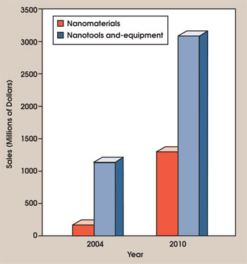
A 20 percent compound annual growth rate is forecast for the nanoelectronics market, largely as a result of demand in construction materials and in theautomotive, industrial chemicals and sporting goods industries.
It examines nanoelectronic device development efforts in five sectors: semiconductors, displays, hard-disk storage, optoelectronics and sensors, and micro-/nanoelectromechanical systems. It presents timelines for commercialization in each of these areas. Nanoelectronic devices in the display industry that are expected to be commercialized in the near term include carbon nanotube backlights and field emission displays, along with polymer and transmission films that use nanomaterials. The market for carbon nanotubes in nanoelectronics is $38 million and is forecast to reach $101 million by 2010.
The report discusses the technical and business requirements that make it difficult for new suppliers to enter the market and challenging for existing ones to remain in it. Inspection and metrology are cited as areas with the greatest potential for equipment suppliers, with market expansion driven by device fabrication as well as by production of materials and characterization of materials. Lithography, deposition and surface conditioning tools also will experience strong growth. It is suggested that the complexity of this market and rapid innovation will result in a need for new partnership models between suppliers and customers so that risks and rewards are shared.
Requirements by application area and definitions for nanomaterials, -tools and -equipment for nanoelectronics are included. Also examined are potential applications in the next five years outside nanoelectronics, such as in the automotive industry, industrial chemicals, sporting goods and construction materials industries, which are predicted to offer the largest growth opportunities for nanomaterials.
Facts and figures in the 53-page report are based on interviews with 138 representatives of manufacturers and suppliers in North America, Asia and Europe. The interviews highlighted the need for a consortium to conduct precompetitive materials research on a worldwide basis to lower development costs and shorten product development cycles.
The report was developed in cooperation with the Semiconductor Industry Association (SIA), also of San Jose, and was issued in November. It sells for $4000 to SEMI and SIA members and $5000 for nonmembers. For more information, call +1 (877) 746-7788 or +1 (408) 943-6901.