Hank Hogan
When it comes to integrated circuit failure analysis, Caesar Saloma of the National Institute of Physics at the University of the Philippines in Quezon City doesn’t blow hot and cold. He’s counting on the circuits to do that.
Saloma, a professor of physics and director of the institute, is working to improve optical techniques for failure analysis. He hopes to use these approaches to identify likely breakdown locations in prototype circuits that cause transistors to run hot from too much current or cold from too little.
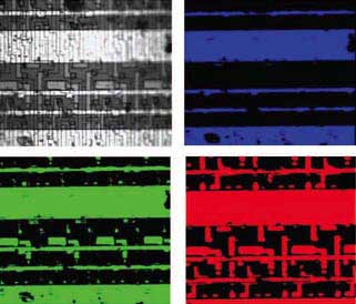
Using thermoreflectance, the change in reflectance due to temperature changes, researchers mapped hot and cold spots on an integrated circuit to find defects. The spectral maps of the reflectance show features at 478, 559 and 641 nm.
The difficulty for optical methods is that transistors are small, densely packed and hard to see. They have feature sizes of about 50 nm, and millions are crammed into an area the size of a thumbnail. Their active area is sandwiched between a bulk silicon substrate hundreds of microns thick and multiple layers of highly reflective metal.
“The technical challenge, therefore, is not only about overcoming the diffraction limit, but also getting enough signal-to-noise ratio for the detected signal,” Saloma said.
Working with engineers from Intel Technology Philippines Inc. in Cavite, the investigators found that they could distinguish broken and leaky transistors using functional infrared emission spectral microscopy. Although the approach is effective, it also is relatively expensive because it employs an infrared CCD camera.
They therefore turned to thermoreflectance, which is based on the relationship between the change in the optical reflection coefficient of a material and the change in its temperature. To test the utility of this method, the scientists used a broadband tungsten source to illuminate an integrated circuit on an X-Y-Z scanning stage from Thorlabs Inc. of Newton, N.J. They ran the reflect light through an ImSpector V9 grating-prism pair spectrometer from Spectral Imaging Ltd. of Oulu, Finland, and they captured the output with a 768 × 493-pixel black and white CCD camera made by Hamamatsu Photonics KK of Hamamatsu, Japan.

Because this type of spectrometer produces data along a line, they had to scan in only one direction to get the total surface of the circuit. Compared with the X and Y stepping that a confocal microscopy-based technique would have required, the method therefore reduced the total testing time.
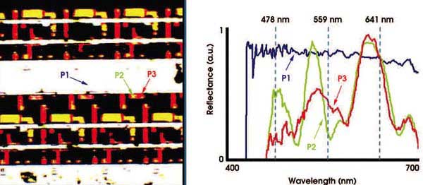
The superimposed spectral maps reveal substructures in the active layer of the circuit. The reflectance spectra show that the structures at two points (P2 and P3) could be distinguished from the differences in the spectra, suggesting that the technique could be used to spot defective circuit components.
The measurement yielded a 400 × 400-pixel reflectance map of the integrated circuit, spanning the 450- to 650-nm wavelength range for each X- and Y-coordinate. Generating a map took approximately three minutes. The investigators did this with the device powered on and off, enabling them to combine the maps into one showing the differences between the two states and revealing those areas of the circuit that were hotter or colder than others.
These temperature variations, Saloma noted, could arise as a result of electrical overstress or of the formation of unwanted generation centers. The former can change the metal layers, while the latter frequently are due to problems in the semiconductor material, such as the presence of an impurity.
In developing ways to ferret out these problems, Saloma hopes to produce a tool or tools that can accurately and economically predict a failure before it happens. He believes that the time-resolved spectral microscopy will achieve this.
Contact: Caesar Saloma, National Institute of Physics, Quezon City, Philippines; +63 2 920 9749; e-mail: [email protected].