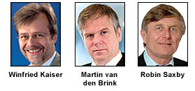
MUNICH, Germany, April 6, 2006 -- Winfried Kaiser of Carl Zeiss SMT AG and Martin van den Brink of ASML received European SEMI (Semiconductor Equipment and Materials International) awards last night at Semicon Europa 2006, being held this week in Munich. They were honored for their leadership in the development of photolithography technology. SEMI also awarded Robin Saxby of ARM with a Special Services Award for his contributions to the European and worldwide processor design industry.
Kaiser is head of product strategy/product development at Carl Zeiss, a Germany-based developer of semiconductor and nanotechnology technology. SEMI said in a statement, "Winfried Kaiser has taken an extremely active role in driving the roadmap for leading-edge lithography tools, and has been a relentless advocate of these tools for chipmakers worldwide. Recognizing the option of water immersion for 193 nm, he helped push the first full field tool for water immersion to market in August 2003, which was followed shortly by the first commercial immersion tools and, ultimately, the first hyper-NA tool."
As a result of Kaiser's work in this area, SEMI said, "there has been a tremendous impact on revenues generated in Europe and worldwide, with end customers generating revenues in the hundreds of billions of euros through the use of these tools."
van den Brink, executive vice president, marketing and technology at ASML, a Netherlands-based provider of lithography systems for the semiconductor industry, began his career there in 1984 as a technical engineer. He was the key engineer in the development of the PAS 5500 stepper platform, the system with which ASML obtained its first large market penetration.
"Martin has demonstrated superior technical expertise, for which he is widely recognized among his peers and ASML customers alike," SEMI said.
Saxby was president and CEO of ARM, a UK based designer of technology for digital, imaging, automotive, security and storage devices until 2001, when he become chairman. Before joining ARM, he worked for companies such as ES2, Motorola Semiconductors and Henderson Security Systems Ltd. Over the years, he has received many industry awards and honorary doctorates; he was knighted 2002.
"All three recipients have made tremendous contributions to advances in technology and helping to establish Europe as a driving force in the worldwide semiconductor industry," said Heinz Kundert, president of SEMI Europe.
For more information, visit: www.semi.org