
Bright LEDs Made on Side Facets of GaN Stripes
Lauren I. Rugani
LEDs are fabricated by growing epitaxial layers along the direction of the crystal polar axis. However, the optical efficiency of these optoelectronic devices decreases with increasing wavelength, due in part to strong internal piezoelectric fields of GaInN quantum wells. Separation of electrons and holes within the wells reduces the probability of radiation recombination. Reducing the piezoelectric fields can overcome this effect, making more efficient luminescence possible.
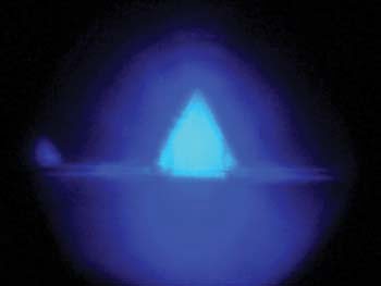
The frontal view of a triangular GaN stripe, imaged with a Zeiss scanning electron microscope, demonstrates the bright blue light emitted by the LED structure.
A solution may be realized by beginning epitaxial growth in the c direction, then using selective epitaxy to form GaN stripes on the side facets where quantum well structures can be grown. A team of researchers at the University of Ulm in Germany has fabricated bright semipolar GaInN/GaN blue LEDs on the semipolar side facets of selectively grown triangular GaN stripes.
The scientists employed low-pressure metallorganic vapor phase epitaxy to grow 1.6-μm-thick GaN templates on c-plane sapphire. These were structured with SiO2 stripes that were oriented in the a direction. On these they grew five GaInN quantum wells and applied a GaN:Mg top layer. The devices had circular mesa structures with diameters between 70 and 140 μm.
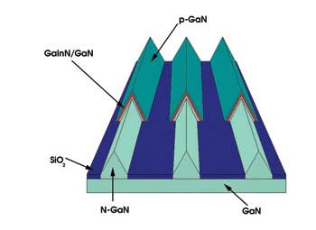
A schematic shows the structural components of the triangular stripes grown on c-plane sapphire. A bigger active area and more effective light outcoupling can be realized as a result of the triangular shape.
The growth behavior of the top layer was dependent on the magnesium fraction and was found to be strongly anisotropic. With magnesium doping, the top layer exhibited preferential lateral growth; without it, vertical growth occurred. Since magnesium is needed for P-type doping of GaN, this resulted in a thin cover layer at the apex of the stripes, increasing the risk of electrical shorting. To resolve this, the researchers developed an electrically isolating Al2O3 coating for the apex. They also found a suitable magnesium fraction to put into the top layer to support more homogeneous growth.
The devices achieved continuous-wave optical output power of 700 μW at 20 mA and up to 3 mW at 110 mA under direct-current operation, a significant improvement over the output power of 240 μW at 20 mA for previous non- or semipolar LED structures. The investigators measured the optical power with an integrating sphere and a calibrated silicon photodiode. The effective emission wavelength of the semipolar facet LEDs — emitting light in the blue spectral range and peaking at 425 nm — experienced a blueshift as the injection current was increased.
For direct currents ranging from 1 to 50 mA, the wavelength shift was 1.5 nm for semipolar LEDs, compared with 3.5 nm for the common polar crystal-plane LEDs. These measurements agree with the researchers’ predicted field reduction of a factor of 2.8 for semipolar facets and confirm a reduced piezoelectric field — and therefore improved electroluminescence — for side facet semipolar LEDs.
Applied Physics Letters, July 24, 2006, 041121.
Published: September 2006